MT36HTF25672PY-667DZES

PDF: 09005aef818e3fc8/Source: 09005aef818e3fdb Micron Technology, Inc., reserves the right to change products or specifications without notice.
HTF36C256_512x72.fm - Rev. C 1/07 EN
10 ©2005 Micron Technology, Inc. All rights reserved.
2GB, 4GB (x72, ECC, DR) 240-Pin DDR2 SDRAM RDIMM
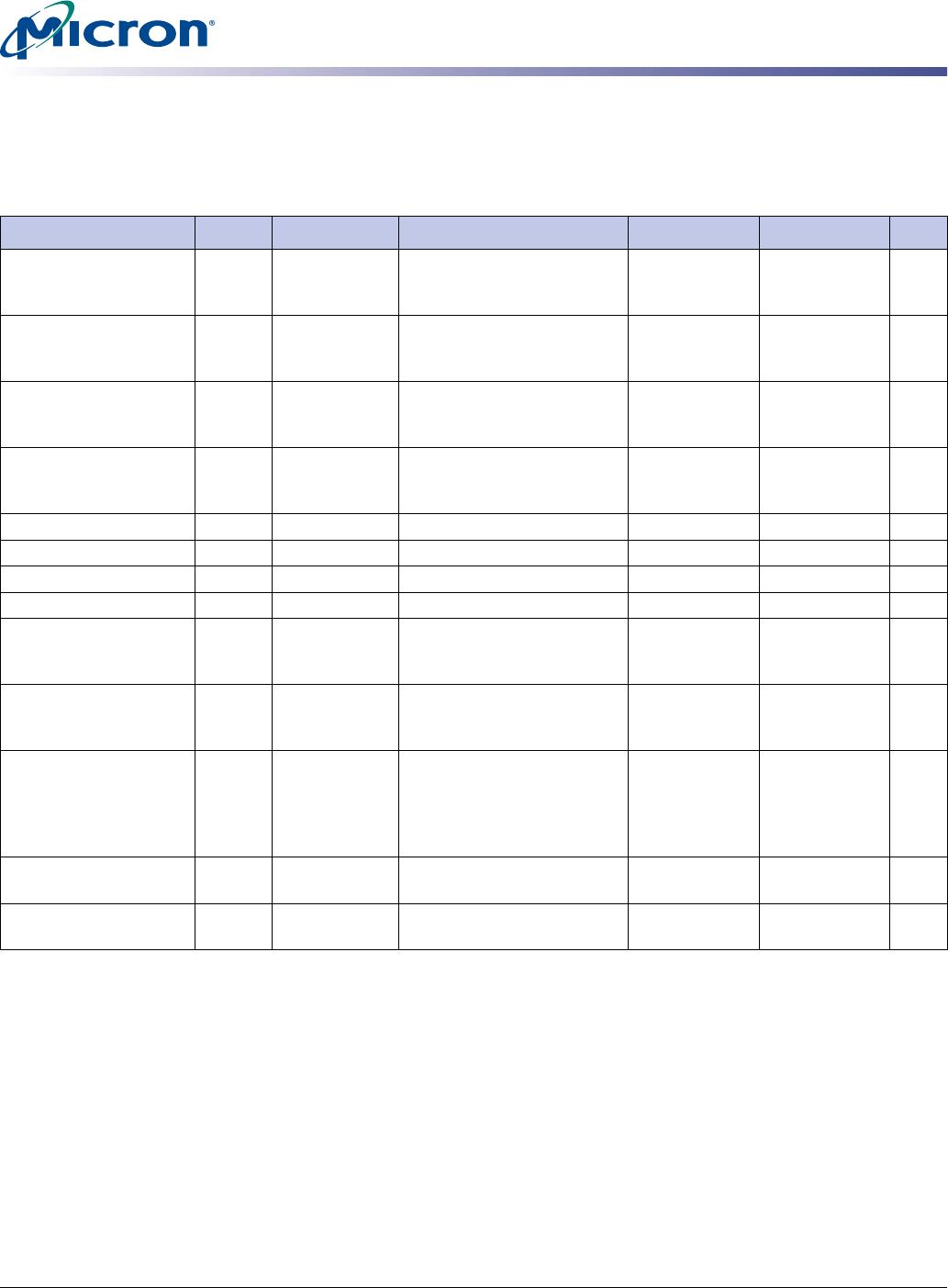
Electrical Specifications
Notes: 1. Value calculated as one module rank in this operating condition, all other module ranks in
I
DD2P (CKE LOW) mode.
2. Value calculated reflects all module ranks in this operating condition.
Table 10: DDR2 IDD Specifications and Conditions – 4GB
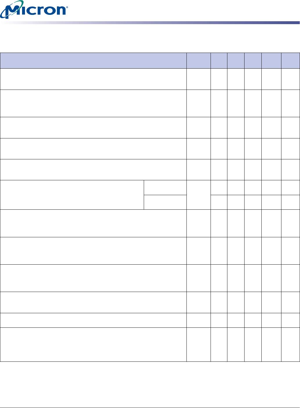
Values shown for MT47H256M4 DDR2 SDRAM only and are computed from values specified in the
1Gb (256 Meg x 4) component data sheet
Parameter/Condition Symbol
-80E
-800
-667 -53E -40E Units
Operating one bank active-precharge current:
t
CK =
t
CK (IDD),
t
RC =
t
RC (IDD),
t
RAS =
t
RAS MIN (IDD); CKE is HIGH, S# is HIGH between valid
commands; Address bus inputs are switching; Data bus inputs are switching
I
DD0
1
1,746 1,656 1,386 1,386 mA
Operating one bank active-read-precharge current: I
OUT = 0mA;
BL = 4, CL = CL (IDD), AL = 0;
t
CK =
t
CK (IDD),
t
RC =
t
RC (IDD),
t
RAS =
t
RAS MIN
(I
DD),
t
RCD =
t
RCD (IDD); CKE is HIGH, S# is HIGH between valid commands;
Address bus inputs are switching; Data pattern is same as IDD4W
I
DD1
1
2,106 1,926 1,836 1,746 mA
Precharge power-down current: All device banks idle;
t
CK =
t
CK (IDD);
CKE is LOW; Other control and address bus inputs are stable; Data bus
inputs are floating
I
DD2P
2
252 252 252 252 mA
Precharge quiet standby current: All device banks idle;
t
CK =
t
CK (IDD);
CKE is HIGH, S# is HIGH; Other control and address bus inputs are stable;
Data bus inputs are floating
IDD2Q
2
1,800 1,440 1,440 1,260 mA
Precharge standby current: All device banks idle;
t
CK =
t
CK (IDD); CKE is
HIGH, S# is HIGH; Other control and address bus inputs are switching; Data
bus inputs are switching
IDD2N
2
1,800 1,440 1,440 1,260 mA
Active power-down current: All device banks open;
t
CK =
t
CK (IDD); CKE is LOW; Other control and address
bus inputs are stable; Data bus inputs are floating
Fast PDN exit
MR[12] = 0
I
DD3P
2
1,440 1,080 1,080 1,080 mA
Slow PDN exit
MR[12] = 1
360 360 360 360 mA
Active standby current: All device banks open;
t
CK =
t
CK (IDD),
t
RAS =
t
RAS MAX (IDD),
t
RP =
t
RP (IDD); CKE is HIGH, S# is HIGH between
valid commands; Other control and address bus inputs are switching; Data
bus inputs are switching
I
DD3N
2
2,160 1,980 1,620 1,440 mA
Operating burst write current: All device banks open; Continuous burst
writes; BL = 4, CL = CL (I
DD), AL = 0;
t
CK =
t
CK (IDD),
t
RAS =
t
RAS MAX (IDD),
t
RP =
t
RP (IDD); CKE is HIGH, S# is HIGH between valid commands; Address
bus inputs are switching; Data bus inputs are switching
I
DD4W
1
3,006 2,556 2,376 2,016 mA
Operating burst read current: All device banks open; Continuous burst
reads, I
OUT = 0mA; BL = 4, CL = CL (IDD), AL = 0;
t
CK =
t
CK (IDD),
t
RAS =
t
RAS
MAX (I
DD),
t
RP =
t
RP (IDD); CKE is HIGH, S# is HIGH between valid
commands; Address bus inputs are switching; Data bus inputs are switching
I
DD4R
1
3,006 2,556 2,376 2,016 mA
Burst refresh current:
t
CK =
t
CK (IDD); REFRESH command at every
t
RFC
(I
DD) interval; CKE is HIGH, S# is HIGH between valid commands; Other
control and address bus inputs are switching; Data bus inputs are switching
I
DD5
2
8,460 7,740 7,560 7,380 mA
Self refresh current: CK and CK# at 0V; CKE 0.2V; Other control and
address bus inputs are floating; Data bus inputs are floating
I
DD6
2
252 252 252 252 mA
Operating bank interleave read current: All device banks interleaving
reads, IOUT = 0mA; BL = 4, CL = CL (IDD), AL =
t
RCD (IDD) - 1 ×
t
CK (IDD);
t
CK =
t
CK (IDD),
t
RC =
t
RC (IDD),
t
RRD =
t
RRD (IDD),
t
RCD =
t
RCD (IDD); CKE is
HIGH, S# is HIGH between valid commands; Address bus inputs are stable
during DESELECTs; Data bus inputs are switching
I
DD7
1
6,156 5,166 4,986 4,806 mA
PDF: 09005aef818e3fc8/Source: 09005aef818e3fdb Micron Technology, Inc., reserves the right to change products or specifications without notice.
HTF36C256_512x72.fm - Rev. C 1/07 EN
11 ©2005 Micron Technology, Inc. All rights reserved.
2GB, 4GB (x72, ECC, DR) 240-Pin DDR2 SDRAM RDIMM
Register and PLL Specifications
Notes: 1. Timing and switching specifications for the register listed above are critical for proper oper-
ation of the DDR2 SDRAM registered DIMMs. These are meant to be a subset of the param-
eters for the specific device used on the module. Detailed information for this register is
available in JEDEC Standard JESD82.
Table 11: Register Specifications
SSTU32868 devices or equivalent JESD82-14 for the 4GB and SSTU32866 devices or equivalent JESD82-10 for
the 2GB
Parameter Symbol Pins Condition Min Max Units
DC high-level
input voltage
V
IH(DC) Address,
control,
command
SSTL_18 VREF(DC) +125 VDDQ + 250 mV
DC low-level
input voltage
VIL(DC) Address,
control,
command
SSTL_18 0 VREF(DC) - 125 mV
AC high-level
input voltage
VIH(AC) Address,
control,
command
SSTL_18 VREF(DC) + 250 VDD mV
AC low-level
input voltage
VIL(AC) Address,
control,
command
SSTL_18 0 VREF(DC) - 250 mV
Output high voltage
VOH Parity output LVCMOS 1.2 mV
Output low voltage
VOL Parity output LVCMOS 0.5 mV
Input current
II All pins VI = VDDQ or VSSQ–5 5µA
Static standby
I
DD All pins RESET# = VSSQ (Io = 0) 100 µA
Static operating
IDD All pins RESET# = VSSQ;
VI = VIH(AC) or VIL(DC)
Io = 0
40mA µA
Dynamic operating –
clock tree
IDDD N/A RESET# = VDD, VI = VIH(AC) or
VIL(AC), Io = 0; CK and CK#
switching 50% duty cycle
–Varies by
manufacturer
µA
Dynamic operating
(per each input)
IDDD N/A RESET# = VDD, VI = VIH(AC) or
VIL(AC), Io = 0; CK and CK#
switching 50% duty cycle;
One data input switching at
t
CK/2, 50% duty cycle
–Varies by
manufacturer
µA
Input capacitance
(per device, per pin)
CI All inputs
except RESET#
VI = VREF ±250mV;
VDDQ = 1.8V
2.5 3.5 pF
Input capacitance
(per device, per pin)
RESET# VI = VDDQ or VSSQ–Varies by
manufacturer
pF
PDF: 09005aef818e3fc8/Source: 09005aef818e3fdb Micron Technology, Inc., reserves the right to change products or specifications without notice.
HTF36C256_512x72.fm - Rev. C 1/07 EN
12 ©2005 Micron Technology, Inc. All rights reserved.
2GB, 4GB (x72, ECC, DR) 240-Pin DDR2 SDRAM RDIMM
Register and PLL Specifications
Notes: 1. PLL timing and switching specifications are critical for proper operation of the DDR2 DIMM.
This is a subset of parameters for the specific PLL used. Detailed PLL information is available
in JEDEC standard JESD82.
Table 12: PLL Specifications
CU877 device or equivalent JESD82-8.01
Parameter Symbol Pins Condition Min Max Units
DC high-level input voltage
V
IH RESET# LVCMOS 0.65 × VDD –mV
DC low-level input voltage
V
IL RESET# LVCMOS 0.35 × VDD mV
Input voltage (limits)
V
IN RESET#, CK, CK# –0.3 VDDQ + 0.3 mV
DC high-level input voltage
VIH CK, CK# Differential input 0.65 × VDD –mV
DC low-level input voltage
V
IL CK, CK# Differential input 0.35 × VDD mV
Input differential-pair cross
voltage
V
IX CK, CK# Differential input (VDDQ/2) -
0.15
(VDDQ/2) +
0.15
V
Input differential voltage
V
ID(DC) CK, CK# Differential input 0.3 VDDQ + 0.4 V
Input differential voltage
V
ID(AC) CK, CK# Differential input 0.6 VDDQ + 0.4 V
Input current
II RESET# VI = VDDQ or VSSQ –10 10 µA
CK, CK# V
I = VDDQ or VSSQ –250 250 µA
Output disabled current
I
ODL RESET# = VSSQ; VI =
V
IH(AC) or VIL(DC)
100 µA
Static supply current
I
DDLD CK = CK# = LOW 500 µA
Dynamic supply
IDD N/A CK, CK# = 270 MHz, all
outputs open
(not connected to PCB)
–300mA
Input capacitance
CIN Each input VI = VDDQ or VSSQ2 3pF
Table 13: PLL Clock Driver Timing Requirements and Switching Characteristics
Parameter Symbol Min Max Units
Stabilization time
t
L–15µs
Input clock slew rate
t
LS
I
1.0 4 V/ns
SSC modulation frequency
30 33 KHz
SSC clock input frequency deviation
0.0 –0.50 %
PLL loop bandwidth (–3dB from unity gain)
2.0 MHz

MT36HTF25672PY-667DZES

Mfr. #:
Manufacturer:
Micron
Description:
MODULE DDR2 SDRAM 2GB 240RDIMM
Lifecycle:
New from this manufacturer.
Delivery:
DHL FedEx Ups TNT EMS
Payment:
T/T Paypal Visa MoneyGram Western Union