1
®
FN9282.1
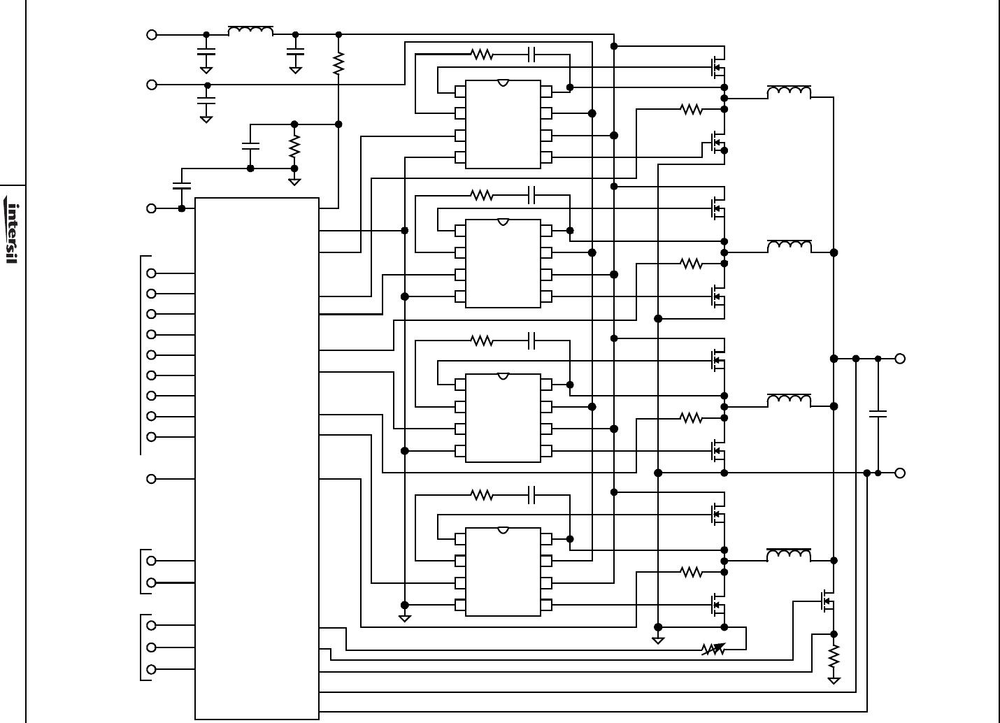
ISL6594D
Advanced Synchronous Rectified Buck
MOSFET Drivers with Protection Features
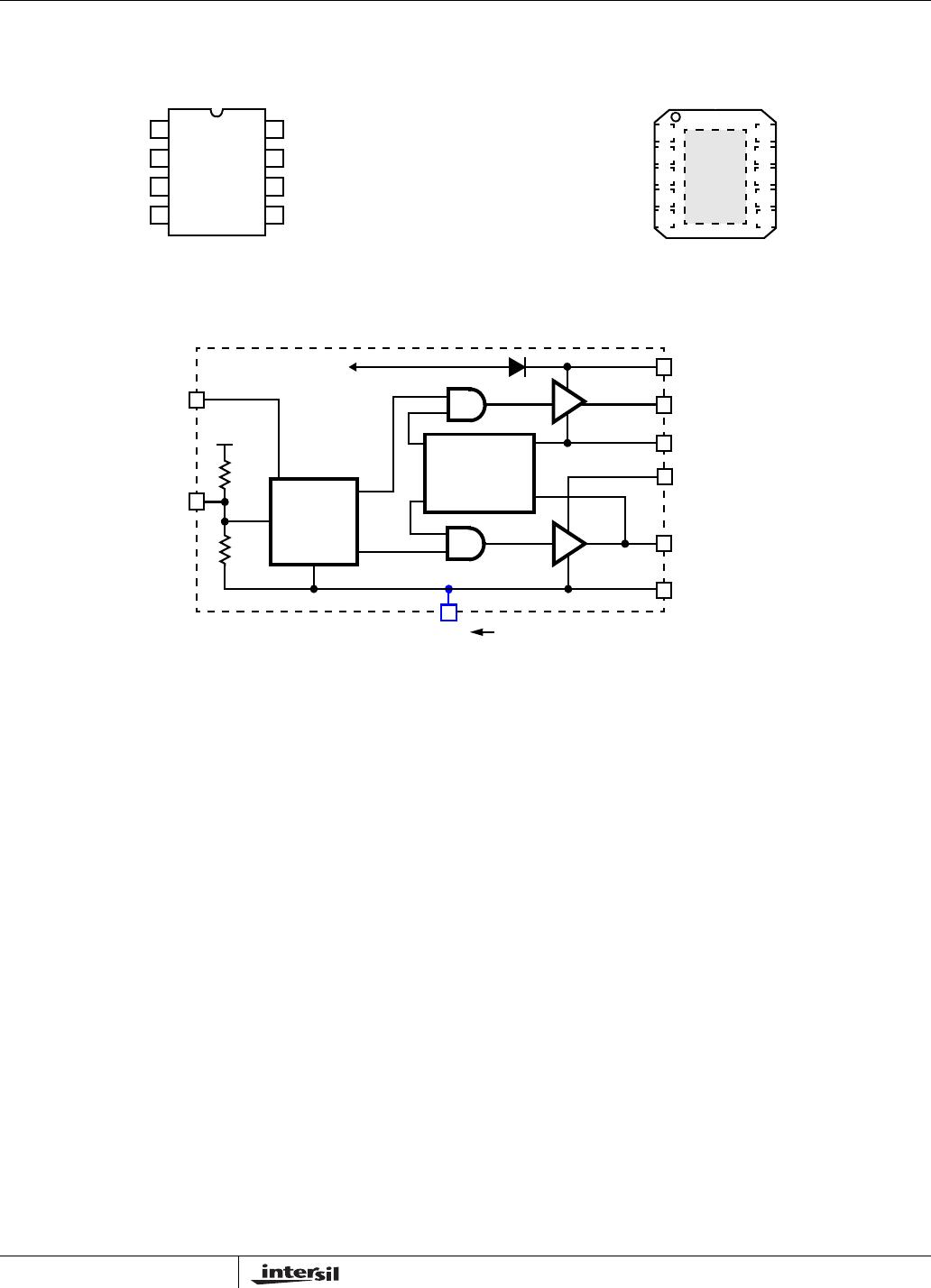
The ISL6594D is high frequency MOSFET driver specifically
designed to drive upper and lower power N-Channel
MOSFETs in a synchronous rectified buck converter
topology. This driver combined with the ISL6594D Digital
Multi-Phase Buck PWM controller and N-Channel MOSFETs
forms a complete core-voltage regulator solution for
advanced microprocessors.
The ISL6594D drives both upper and lower gates over a range
of 4.5V to 13.2V. This drive-voltage provides the flexibility
necessary to optimize applications involving trade-offs between
gate charge and conduction losses.
An advanced adaptive zero shoot-through protection is
integrated to prevent both the upper and lower MOSFETs
from conducting simultaneously and to minimize the dead
time. The ISL6594D includes an overvoltage protection
feature operational before VCC exceeds its turn-on
threshold, at which the PHASE node is connected to the
gate of the low side MOSFET (LGATE). The output voltage
of the converter is then limited by the threshold of the low
side MOSFET, which provides some protection to the
microprocessor if the upper MOSFET(s) is shorted.
The ISL6594D also features an input that recognizes a
high-impedance state, working together with Intersil multi-
phase PWM controllers to prevent negative transients on the
controlled output voltage when operation is suspended. This
feature eliminates the need for the Schottky diode that may
be utilized in a power system to protect the load from
negative output voltage damage.
Features
• Dual MOSFET Drives for Synchronous Rectified Bridge
• Pin-to-pin Compatible with ISL6596
• Advanced Adaptive Zero Shoot-Through Protection
- Body Diode Detection
- Auto-zero of r
DS(ON)
Conduction Offset Effect
• Adjustable Gate Voltage for Optimal Efficiency
• 36V Internal Bootstrap Schottky Diode
• Bootstrap Capacitor Overcharging Prevention
• Supports High Switching Frequency (up to 2MHz)
- 3A Sinking Current Capability
- Fast Rise/Fall Times and Low Propagation Delays
• Optimized for 3.3V PWM Input
• Three-State PWM Input for Output Stage Shutdown
• Three-State PWM Input Hysteresis for Applications With
Power Sequencing Requirement
• Pre-POR Overvoltage Protection
• VCC Undervoltage Protection
• Expandable Bottom Copper Pad for Enhanced Heat
Sinking
• Dual Flat No-Lead (DFN) Package
- Near Chip-Scale Package Footprint; Improves PCB
Efficiency and Thinner in Profile
• Pb-Free (RoHS Compliant)
Applications
• Optimized for POL DC/DC Converters for IBA Systems
• Core Regulators for Intel® and AMD® Microprocessors
• High Current DC/DC Converters
• High Frequency and High Efficiency VRM and VRD
Related Literature
Technical Brief TB363 “Guidelines for Handling and
Processing Moisture Sensitive Surface Mount Devices
(SMDs)”
Technical Brief TB389 “PCB Land Pattern Design and
Surface Mount Guidelines for QFN (MLFP) Packages”
Ordering Information
PART NUMBER
(Note)
PART
MARKING
TEMP.
RANGE (°C)
PACKAGE
(Pb-free)
PKG.
DWG. #
ISL6594DCBZ 6594 DCBZ 0 to +85 8 Ld SOIC M8.15
ISL6594DCBZ-T* 6594 DCBZ 0 to +85 8 Ld SOIC
Tape and Reel
M8.15
ISL6594DCRZ 94DZ 0 to +85 10 Ld 3x3 DFN L10.3x3
ISL6594DCRZ-T* 94DZ 0 to +85 10 Ld 3x3 DFN
Tape and Reel
L10.3x3
*Please refer to TB347 for details on reel specifications.
NOTE: These Intersil Pb-free plastic packaged products employ
special Pb-free material sets; molding compounds/die attach
materials and 100% matte tin plate PLUS ANNEAL - e3 termination
finish, which is RoHS compliant and compatible with both SnPb and
Pb-free soldering operations. Intersil Pb-free products are MSL
classified at Pb-free peak reflow temperatures that meet or exceed the
Pb-free requirements of IPC/JEDEC J STD-020.
Data Sheet December 3, 2007
CAUTION: These devices are sensitive to electrostatic discharge; follow proper IC Handling Procedures.
1-888-INTERSIL or 1-888-468-3774
| Intersil (and design) is a registered trademark of Intersil Americas Inc.
Copyright Intersil Americas Inc. 2006, 2007. All Rights Reserved
All other trademarks mentioned are the property of their respective owners.