ISL6594DCRZ-T

4
FN9282.1
December 3, 2007
Absolute Maximum Ratings Thermal Information
Supply Voltage (VCC) . . . . . . . . . . . . . . . . . . . . . . . . . . . . . . . . .15V
Supply Voltage (PVCC) . . . . . . . . . . . . . . . . . . . . . . . . . VCC + 0.3V
BOOT Voltage (V
BOOT-GND
). . . . . . . . . . . . . . . . . . . . . . . . . . . .36V
Input Voltage (V
PWM
) . . . . . . . . . . . . . . . . . . . . . . GND - 0.3V to 7V
UGATE. . . . . . . . . . . . . . . . . . . V
PHASE
- 0.3V
DC
to V
BOOT
+ 0.3V
V
PHASE
- 3.5V (<100ns Pulse Width, 2µJ) to V
BOOT
+ 0.3V
LGATE . . . . . . . . . . . . . . . . . . . . . . GND - 0.3V
DC
to V
PVCC
+ 0.3V
GND - 5V (<100ns Pulse Width, 2µJ) to V
PVCC
+ 0.3V
PHASE. . . . . . . . . . . . . . . . . . . . . . . . . . . . GND - 0.3V
DC
to 15V
DC
GND - 8V (<400ns, 20µJ) to 30V (<200ns, V
BOOT-GND
<36V))
ESD Rating
Human Body Model . . . . . . . . . . . . . . . . . . . . Class I JEDEC STD
Thermal Resistance θ
JA
(°C/W) θ
JC
(°C/W)
SOIC Package (Note 1) . . . . . . . . . . . . 100 N/A
DFN Package (Notes 2, 3). . . . . . . . . . 48 7
Maximum Junction Temperature (Plastic Package) . . . . . . . +150°C
Maximum Storage Temperature Range. . . . . . . . . .-65°C to +150°C
Pb-free reflow profile . . . . . . . . . . . . . . . . . . . . . . . . . .see link below
http://www.intersil.com/pbfree/Pb-FreeReflow.asp
Recommended Operating Conditions
Ambient Temperature Range. . . . . . . . . . . . . . . . . . . . 0°C to +85°C
Maximum Operating Junction Temperature. . . . . . . . . . . . . +125°C
Supply Voltage, V
CC
. . . . . . . . . . . . . . . . . . . . . . . . . . 6.8V to 13.2V
Supply Voltage Range, PVCC . . . . . . . . . . . . . . . . 5V to 12V ±10%
CAUTION: Do not operate at or near the maximum ratings listed for extended periods of time. Exposure to such conditions may adversely impact product reliability and
result in failures not covered by warranty.
NOTES:
1. θ
JA
is measured with the component mounted on a high effective thermal conductivity test board in free air.
2. θ
JA
is measured in free air with the component mounted on a high effective thermal conductivity test board with “direct attach” features. See
Tech Brief TB379.
3. For θ
JC
, the “case temp” location is the center of the exposed metal pad on the package underside.
Electrical Specifications Recommended Operating Conditions, Unless Otherwise Noted.
PARAMETER SYMBOL TEST CONDITIONS MIN TYP MAX UNITS
VCC SUPPLY CURRENT
Bias Supply Current I
VCC
ISL6594D, f
PWM
= 300kHz, V
VCC
= 12V - 4.5 - mA
I
VCC
ISL6594D, f
PWM
= 1MHz, V
VCC
= 12V - 5 - mA
Gate Drive Bias Current I
PVCC
ISL6594D, f
PWM
= 300kHz, V
PVCC
= 12V - 7.5 - mA
I
PVCC
ISL6594D, f
PWM
= 1MHz, V
PVCC
= 12V - 8.5 - mA
POWER-ON RESET AND ENABLE
VCC Rising Threshold 6.1 6.4 6.7 V
VCC Falling Threshold 4.7 5.0 5.3 V
PWM INPUT (See Timing Diagram on page 6)
Input Current I
PWM
V
PWM
= 3.3V - 400 - µA
V
PWM
= 0V - -350 - µA
PWM Rising Threshold (Note 4) V
CC
= 12V - 1.70 - V
PWM Falling Threshold (Note 4) V
CC
= 12V - 1.30 - V
Typical Three-State Shutdown Window V
CC
= 12V 1.23 - 1.82 V
Three-State Lower Gate Falling Threshold V
CC
= 12V - 1.18 - V
Three-State Lower Gate Rising Threshold V
CC
= 12V - 0.76 - V
Three-State Upper Gate Rising Threshold V
CC
= 12V - 2.36 - V
Three-State Upper Gate Falling Threshold V
CC
= 12V - 1.96 - V
Shutdown Hold-off Time t
TSSHD
- 245 - ns
UGATE Rise Time (Note 4) t
RU
V
PVCC
= 12V, 3nF Load, 10% to 90% - 26 - ns
LGATE Rise Time (Note 4) t
RL
V
PVCC
= 12V, 3nF Load, 10% to 90% - 18 - ns
UGATE Fall Time (Note 4) t
FU
V
PVCC
= 12V, 3nF Load, 90% to 10% - 18 - ns
LGATE Fall Time (Note 4) t
FL
V
PVCC
= 12V, 3nF Load, 90% to 10% - 12 - ns
UGATE Turn-On Propagation Delay (Note 4) t
PDHU
V
PVCC
= 12V, 3nF Load, Adaptive - 10 - ns
ISL6594D
5
FN9282.1
December 3, 2007
LGATE Turn-On Propagation Delay (Note 4) t
PDHL
V
PVCC
= 12V, 3nF Load, Adaptive - 10 - ns
UGATE Turn-Off Propagation Delay (Note 4) t
PDLU
V
PVCC
= 12V, 3nF Load - 10 - ns
LGATE Turn-Off Propagation Delay (Note 4) t
PDLL
V
PVCC
= 12V, 3nF Load - 10 - ns
LG/UG Three-State Propagation Delay (Note 4) t
PDTS
V
PVCC
= 12V, 3nF Load - 10 - ns
OUTPUT (Note 4)
Upper Drive Source Current I
U_SOURCE
V
PVCC
= 12V, 3nF Load - 1.25 - A
Upper Drive Source Impedance R
U_SOURCE
150mA Source Current 1.4 2.0 3.0 Ω
Upper Drive Sink Current I
U_SINK
V
PVCC
= 12V, 3nF Load - 2 - A
Upper Drive Sink Impedance R
U_SINK
150mA Sink Current 0.9 1.65 3.0 Ω
Lower Drive Source Current I
L_SOURCE
V
PVCC
= 12V, 3nF Load - 2 - A
Lower Drive Source Impedance R
L_SOURCE
150mA Source Current 0.85 1.3 2.2 Ω
Lower Drive Sink Current I
L_SINK
V
PVCC
= 12V, 3nF Load - 3 - A
Lower Drive Sink Impedance R
L_SINK
150mA Sink Current 0.60 0.94 1.35 Ω
NOTE:
4. Limits should be considered typical and are not production tested.
Electrical Specifications Recommended Operating Conditions, Unless Otherwise Noted. (Continued)
PARAMETER SYMBOL TEST CONDITIONS MIN TYP MAX UNITS
Functional Pin Description
PACKAGE PIN #
PIN
SYMBOL FUNCTIONSOIC DFN
1 1 UGATE Upper gate drive output. Connect to gate of high-side power N-Channel MOSFET.
2 2 BOOT Floating bootstrap supply pin for the upper gate drive. Connect the bootstrap capacitor between this pin and the
PHASE pin. The bootstrap capacitor provides the charge to turn on the upper MOSFET. See “Internal Bootstrap
Device” on page 7 for guidance in choosing the capacitor value.
- 3, 8 N/C No Connection.
3 4 PWM The PWM signal is the control input for the driver. The PWM signal can enter three distinct states during operation, see
Three-State PWM Input” on page 6 for further details. Connect this pin to the PWM output of the controller.
4 5 GND Bias and reference ground. All signals are referenced to this node. It is also the power ground return of the driver.
5 6 LGATE Lower gate drive output. Connect to gate of the low-side power N-Channel MOSFET.
6 7 VCC Its operating range is +6.8V to 13.2V. Place a high quality low ESR ceramic capacitor from this pin to GND.
7 9 PVCC This pin supplies power to both upper and lower gate drives. Its operating range is +4.5V to 13.2V. Place a high
quality low ESR ceramic capacitor from this pin to GND.
8 10 PHASE Connect this pin to the SOURCE of the upper MOSFET and the DRAIN of the lower MOSFET. This pin provides
a return path for the upper gate drive.
9 11 PAD Connect this pad to the power ground plane (GND) via thermally enhanced connection.
ISL6594D
6
FN9282.1
December 3, 2007
Description
Operation
Designed for versatility and speed, the ISL6594D MOSFET
driver controls both high-side and low-side N-Channel FETs
of a half-bridge power train from one externally provided
PWM signal.
Prior to VCC exceeding its POR level, the Pre-POR
overvoltage protection function is activated during initial
start-up; the upper gate (UGATE) is held low and the lower
gate (LGATE), controlled by the Pre-POR overvoltage
protection circuits, is connected to the PHASE. Once the
VCC voltage surpasses the VCC Rising Threshold (see
“Electrical Specifications” on page 4), the PWM signal takes
control of gate transitions. A rising edge on PWM initiates
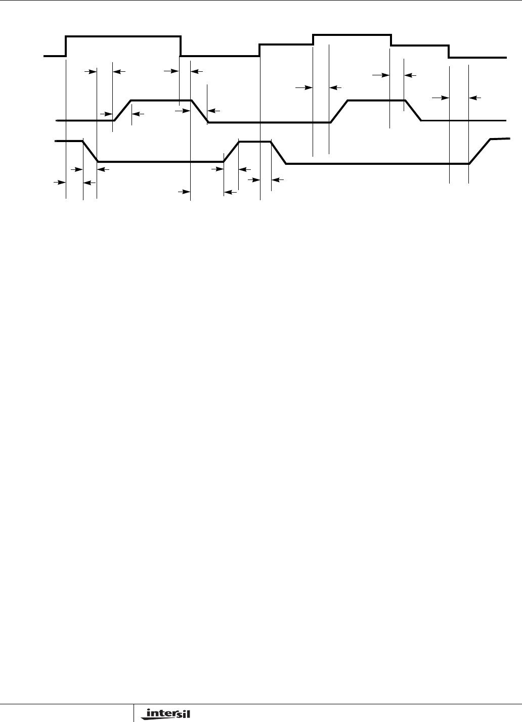
the turn-off of the lower MOSFET (see Timing Diagram on
page 6). After a short propagation delay [t
PDLL
], the lower
gate begins to fall. Typical fall times [t
FL
] are provided in the
“Electrical Specifications” on page 4. Adaptive shoot-through
circuitry monitors the LGATE voltage and determines the
upper gate delay time [t
PDHU
]. This prevents both the lower
and upper MOSFETs from conducting simultaneously. Once
this delay period is complete, the upper gate drive begins to
rise [t
RU
] and the upper MOSFET turns on.
A falling transition on PWM results in the turn-off of the upper
MOSFET and the turn-on of the lower MOSFET. A short
propagation delay [t
PDLU
] is encountered before the upper
gate begins to fall [t
FU
]. Again, the adaptive shoot-through
circuitry determines the lower gate delay time, t
PDHL
. The
PHASE voltage and the UGATE voltage are monitored, and
the lower gate is allowed to rise after PHASE drops below a
level or the voltage of UGATE to PHASE reaches a level
depending upon the current direction (See next section for
details). The lower gate then rises [t
RL
], turning on the lower
MOSFET.
Advanced Adaptive Zero Shoot-Through Deadtime
Control (Patent Pending)
The ISL6594D driver incorporates a unique adaptive
deadtime control technique to minimize deadtime, resulting
in high efficiency from the reduced freewheeling time of the
lower MOSFETs’ body-diode conduction, and to prevent the
upper and lower MOSFETs from conducting simultaneously.
This is accomplished by ensuring either rising gate turns on
its MOSFET with minimum and sufficient delay after the
other has turned off.
During turn-off of the lower MOSFET, the PHASE voltage is
monitored until it reaches a -0.2V/+0.8V trip point within
15ns for a forward/reverse current, at which time the UGATE
turns on after 10ns propagation delay. An auto-zero
comparator is used to correct the r
DS(ON)
drop in the phase
voltage preventing from false detection of the -0.2V phase
level during r
DS(ON)
conduction period. In the case of zero
current and/or 15ns phase detect expired, the UGATE turns
on after 10ns propagation delay. During the phase detection,
the disturbance of LGATE’s falling transition on the PHASE
node is blanked out to prevent falsely tripping. Once the
PHASE is high, the advanced adaptive shoot-through
circuitry monitors the PHASE and UGATE voltages during a
PWM falling edge and the subsequent UGATE turn-off. If
either the UGATE falls to less than 1.75V above the PHASE
or the PHASE falls to less than +0.8V, the LGATE is
released to turn on after 10ns propagation delay.
Three-State PWM Input
A unique feature of these drivers and other Intersil drivers is
the addition of a shutdown window to the PWM input. If the
PWM signal enters and remains within the shutdown window
for a set hold-off time, the driver outputs are disabled and
both MOSFET gates are pulled and held low. The shutdown
state is removed when the PWM signal moves outside the
shutdown window. Otherwise, the PWM rising and falling
PWM
UGATE
LGATE
t
FL
t
PDHU
t
PDLL
t
RL
t
TSSHD
t
PDTS
t
PDTS
1.18V < PWM < 2.36V
0.76V < PWM < 1.96V
t
FU
t
RU
t
PDLU
t
PDHL
t
TSSHD
FIGURE 1. TIMING DIAGRAM
ISL6594D

ISL6594DCRZ-T

Mfr. #:
Manufacturer:
Renesas / Intersil
Description:
Gate Drivers SYNCH BUCK FET DRVR W/3 3V PWM LW POR
Lifecycle:
New from this manufacturer.
Delivery:
DHL FedEx Ups TNT EMS
Payment:
T/T Paypal Visa MoneyGram Western Union

Products related to this Datasheet