ISL6594DCRZ-T

7
FN9282.1
December 3, 2007
thresholds outlined in the “Electrical Specifications” on
page 4 determine when the lower and upper gates are
enabled.
This feature helps prevent a negative transient on the output
voltage when the output is shut down, eliminating the
Schottky diode that is used in some systems for protecting
the load from reversed output voltage events.
In addition, more than 400mV hysteresis also incorporates
into the three-state shutdown window to eliminate PWM
input oscillations due to the capacitive load seen by the
PWM input through the body diode of the controller’s PWM
output when the power-up and/or power-down sequence of
bias supplies of the driver and PWM controller are required.
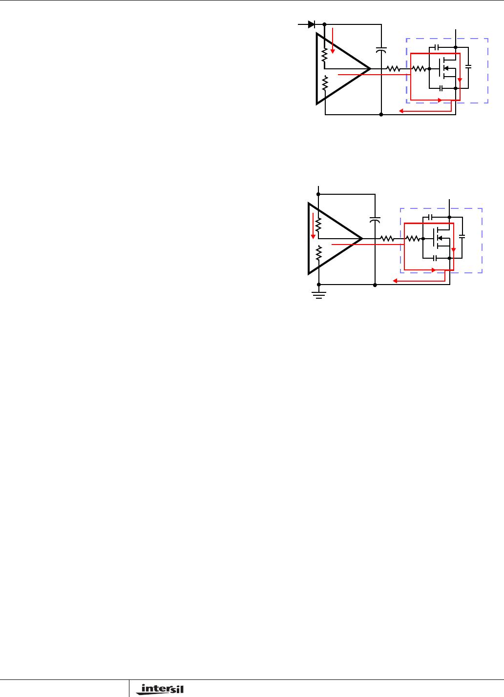
Power-On Reset (POR) Function
During initial start-up, the VCC voltage rise is monitored.
Once the rising VCC voltage exceeds 6.4V (typically),
operation of the driver is enabled and the PWM input signal
takes control of the gate drives. If VCC drops below the
falling threshold of 5.0V (typically), operation of the driver is
disabled.
Pre-POR Overvoltage Protection
Prior to VCC exceeding its POR level, the upper gate is held
low and the lower gate is controlled by the overvoltage
protection circuits. The upper gate driver is powered from
PVCC and will be held low when a voltage of 2.75V or higher
is present on PVCC as VCC surpasses its POR threshold.
The PHASE is connected to the gate of the low side
MOSFET (LGATE), which provides some protection to the
microprocessor if the upper MOSFET(s) is shorted during
start-up, normal, or shutdown conditions. For complete
protection, the low side MOSFET should have a gate
threshold well below the maximum voltage rating of the
load/microprocessor.
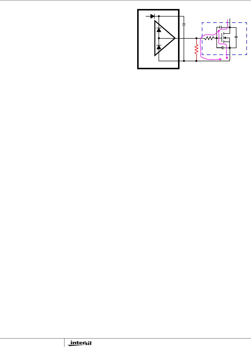
Internal Bootstrap Device
Both drivers feature an internal bootstrap Schottky diode.
Simply adding an external capacitor across the BOOT and
PHASE pins completes the bootstrap circuit. The bootstrap
function is also designed to prevent the bootstrap capacitor
from overcharging due to the large negative swing at the
trailing-edge of the PHASE node. This reduces voltage
stress on the boot to phase pins.
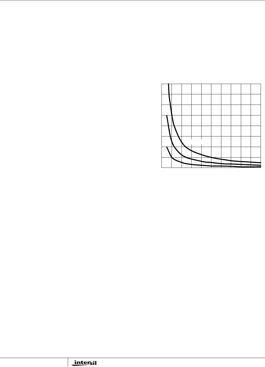
The bootstrap capacitor must have a maximum voltage
rating above PVCC + 5V and its capacitance value can be
chosen from Equation 1:
where Q
G1
is the amount of gate charge per upper MOSFET
at V
GS1
gate-source voltage and N
Q1
is the number of
control MOSFETs. The DV
BOOT_CAP
term is defined as the
allowable droop in the rail of the upper gate drive.
As an example, suppose two IRLR7821 FETs are chosen as
the upper MOSFETs. The gate charge, Q
G
, from the data
sheet is 10nC at 4.5V (V
GS
) gate-source voltage. Then the
Q
GATE
is calculated to be 53nC for PVCC = 12V. We will
assume a 200mV droop in drive voltage over the PWM
cycle. We find that a bootstrap capacitance of at least
0.267
µF is required.
Gate Drive Voltage Versatility
The ISL6594D provides the user flexibility in choosing the
gate drive voltage for efficiency optimization. The ISL6594D
ties the upper and lower drive rails together. Simply applying
a voltage from +4.5V up to 13.2V on PVCC sets both gate
drive rail voltages simultaneously, while VCC’s operating
range is from +6.8V up to 13.2V. For 5V operation,
ISL6596/ISL6609 is recommended.
Power Dissipation
Package power dissipation is mainly a function of the
switching frequency (f
SW
), the output drive impedance, the
external gate resistance, and the selected MOSFET’s internal
gate resistance and total gate charge. Calculating the power
dissipation in the driver for a desired application is critical to
ensure safe operation. Exceeding the maximum allowable
power dissipation level will push the IC beyond the maximum
recommended operating junction temperature of +125°C. The
maximum allowable IC power dissipation for the SO8 package
is approximately 800mW at room temperature, while the
power dissipation capacity in the DFN package, with an
exposed heat escape pad, is more than 1.5W. The DFN
package is more suitable for high frequency applications. See
Layout Considerations” on page 8 for thermal transfer
C
BOOT_CAP
Q
GATE
ΔV
BOOT_CAP
--------------------------------------
Q
GATE
Q
G1
PVCC
V
GS1
------------------------------------
N
Q1
=
(EQ. 1)
50nC
20nC
FIGURE 2. BOOTSTRAP CAPACITANCE vs BOOT RIPPLE
VOLTAGE
ΔV
BOOT_CAP
(V)
C
BOOT_CAP
(µF)
1.6
1.4
1.2
1.0
0.8
0.6
0.4
0.2
0.0
0.30.0 0.1 0.2 0.4 0.5 0.6 0.90.7 0.8 1.0
Q
GATE
= 100nC
ISL6594D
8
FN9282.1
December 3, 2007
improvement suggestions. When designing the driver into an
application, it is recommended that the following calculations
are used to ensure safe operation at the desired frequency for
the selected MOSFETs. The total gate drive power losses due
to the gate charge of MOSFETs and the driver’s internal
circuitry and their corresponding average driver current can
be estimated with Equations 2 and 3, respectively:
where the gate charge (Q
G1
and Q
G2
) is defined at a
particular gate to source voltage (V
GS1
and V
GS2
) in the
corresponding MOSFET datasheet; I
Q
is the driver’s total
quiescent current with no load at both drive outputs; N
Q1
and N
Q2
are number of upper and lower MOSFETs,
respectively; PVCC is the drive voltage for both upper and
lower FETs. The I
Q*
VCC product is the quiescent power of
the driver without capacitive load and is typically 116mW at
300kHz and VCC = PVCC = 12V.
The total gate drive power losses are dissipated among the
resistive components along the transition path. The drive
resistance dissipates a portion of the total gate drive power
losses, the rest will be dissipated by the external gate
resistors (R
G1
and R
G2
) and the internal gate resistors
(R
GI1
and R
GI2
) of MOSFETs. Figures 3 and 4 show the
typical upper and lower gate drives turn-on transition path.
The power dissipation on the driver can be roughly
estimated as:
Application Information
Layout Considerations
The parasitic inductances of the PCB and of the power
devices’ packaging (both upper and lower MOSFETs) can
cause serious ringing, exceeding absolute maximum rating
of the devices. Careful layout can help minimize such
unwanted stress. The following advice is meant to lead to an
optimized layout:
Keep decoupling loops (PVCC-GND and BOOT-PHASE)
as short as possible.
Minimize trace inductance, especially on low-impedance
lines. All power traces (UGATE, PHASE, LGATE, GND,
PVCC) should be short and wide, as much as possible.
Minimize the inductance of the PHASE node. Ideally, the
source of the upper and the drain of the lower MOSFET
should be as close as thermally allowable.
Minimize the current loop of the output and input power
trains. Short the source connection of the lower MOSFET
to ground as close to the transistor pin as feasible. Input
capacitors (especially ceramic decoupling) should be
placed as close to the drain of upper and source of lower
MOSFETs as possible.
In addition, for heat spreading, place copper underneath the
IC whether it has an exposed pad or not. The copper area
can be extended beyond the bottom area of the IC and/or
connected to buried power ground plane(s) with thermal
P
Qg_TOT
P
Qg_Q1
P
Qg_Q2
I
Q
VCC++=
(EQ. 2)
P
Qg_Q1
Q
G1
PVCC
2
V
GS1
---------------------------------------
f
SW
N
Q1
=
P
Qg_Q2
Q
G2
PVCC
2
V
GS2
---------------------------------------
f
SW
N
Q2
=
I
DR
Q
G1
PVCC N
Q1
V
GS1
-----------------------------------------------------
Q
G2
PVCC N
Q2
V
GS2
-----------------------------------------------------
+
⎝⎠
⎜⎟
⎛⎞
f
SW
I
Q
+=
(EQ. 3)
P
DR
P
DR_UP
P
DR_LOW
I
Q
VCC++=
(EQ. 4)
P
DR_UP
R
HI1
R
HI1
R
EXT1
+
--------------------------------------
R
LO1
R
LO1
R
EXT1
+
----------------------------------------
+
⎝⎠
⎜⎟
⎛⎞
P
Qg_Q1
2
---------------------
=
P
DR_LOW
R
HI2
R
HI2
R
EXT2
+
--------------------------------------
R
LO2
R
LO2
R
EXT2
+
----------------------------------------
+
⎝⎠
⎜⎟
⎛⎞
P
Qg_Q2
2
---------------------
=
R
EXT1
R
G1
R
GI1
N
Q1
-------------
+=
R
EXT2
R
G2
R
GI2
N
Q2
-------------
+=
FIGURE 3. TYPICAL UPPER-GATE DRIVE TURN-ON PATH
FIGURE 4. TYPICAL LOWER-GATE DRIVE TURN-ON PATH
Q1
D
S
G
R
GI1
R
G1
BOOT
R
HI1
C
DS
C
GS
C
GD
R
LO1
PHASE
PVCC
PVCC
Q2
D
S
G
R
GI2
R
G2
R
HI2
C
DS
C
GS
C
GD
R
LO2
ISL6594D
9
FN9282.1
December 3, 2007
vias. This combination of vias for vertical heat escape,
extended copper plane, and buried planes for heat
spreading allows the IC to achieve its full thermal potential.
Upper MOSFET Self Turn-On Effects at Start-up
Should the driver have insufficient bias voltage applied, its
outputs are floating. If the input bus is energized at a high
dV/dt rate while the driver outputs are floating, because of
self-coupling via the internal C
GD
of the MOSFET, the
UGATE could momentarily rise up to a level greater than the
threshold voltage of the MOSFET. This could potentially turn
on the upper switch and result in damaging inrush energy.
Therefore, if such a situation (when input bus powered up
before the bias of the controller and driver is ready) could
conceivably be encountered, it is a common practice to
place a resistor (R
UGPH
) across the gate and source of the
upper MOSFET to suppress the Miller coupling effect. The
value of the resistor depends mainly on the input voltage’s
rate of rise, the C
GD
/C
GS
ratio, as well as the gate-source
threshold of the upper MOSFET. A higher dV/dt, a lower
C
DS
/C
GS
ratio, and a lower gate-source threshold upper
FET will require a smaller resistor to diminish the effect of
the internal capacitive coupling. For most applications, a
5kΩ to 10kΩ resistor is typically sufficient, not affecting
normal performance and efficiency.
The coupling effect can be roughly estimated using
Equation 5, which assume a fixed linear input ramp and
neglect the clamping effect of the body diode of the upper
drive and the bootstrap capacitor. Other parasitic
components such as lead inductances and PCB
capacitances are also not taken into account. These
equations are provided for guidance purpose only.
Therefore, the actual coupling effect should be examined
using a very high impedance (10MΩ or greater) probe to
ensure a safe design margin.
V
GS_MILLER
dV
dt
-------
RC
rss
1e
V
DS
dV
dt
-------
RC
iss
----------------------------------
⎝⎠
⎜⎟
⎜⎟
⎜⎟
⎜⎟
⎛⎞
⋅⋅=
RR
UGPH
R
GI
+=
C
rss
C
GD
=
C
iss
C
GD
C
GS
+=
(EQ. 5)
FIGURE 5. GATE TO SOURCE RESISTOR TO REDUCE
UPPER MOSFET MILLER COUPLING
VIN
Q
UPPER
D
S
G
R
GI
R
UGPH
BOOT
DU
C
DS
C
GS
C
GD
DL
PHASE
PVCC
ISL6594D
C
BOOT
UGATE
ISL6594D

ISL6594DCRZ-T

Mfr. #:
Manufacturer:
Renesas / Intersil
Description:
Gate Drivers SYNCH BUCK FET DRVR W/3 3V PWM LW POR
Lifecycle:
New from this manufacturer.
Delivery:
DHL FedEx Ups TNT EMS
Payment:
T/T Paypal Visa MoneyGram Western Union

Products related to this Datasheet