DS027 (v3.5) June 25, 2008 www.xilinx.com
Product Specification 1
© Copyright 1998-2008 Xilinx, Inc. XILINX, the Xilinx logo, Virtex, Spartan, ISE and other designated brands included herein are trademarks of Xilinx in the United States and
other countries. All other trademarks are the property of their respective owners.
Features
One-time programmable (OTP) read-only memory
designed to store configuration bitstreams of Xilinx
®
FPGAs
Simple interface to the FPGA; requires only one user
I/O pin
Cascadable for storing longer or multiple bitstreams
Programmable reset polarity (active High or active
Low) for compatibility with different FPGA solutions
XC17128E/EL, XC17256E/EL, XC1701, and XC1700L
series support fast configuration
Low-power CMOS floating-gate process
XC1700E series are available in 5V and 3.3V versions
XC1700L series are available in 3.3V only
Available in compact plastic packages: 8-pin SOIC, 8-
pin VOIC, 8-pin PDIP, 20-pin SOIC, 20-pin PLCC, 44-
pin PLCC or 44-pin VQFP
Programming support by leading programmer
manufacturers
Design support using the Xilinx Alliance and
Foundation™ software packages
Guaranteed 20 year life data retention
Lead-free (Pb-free) packaging available
Description
The XC1700 family of configuration PROMs provides an
easy-to-use, cost-effective method for storing large Xilinx
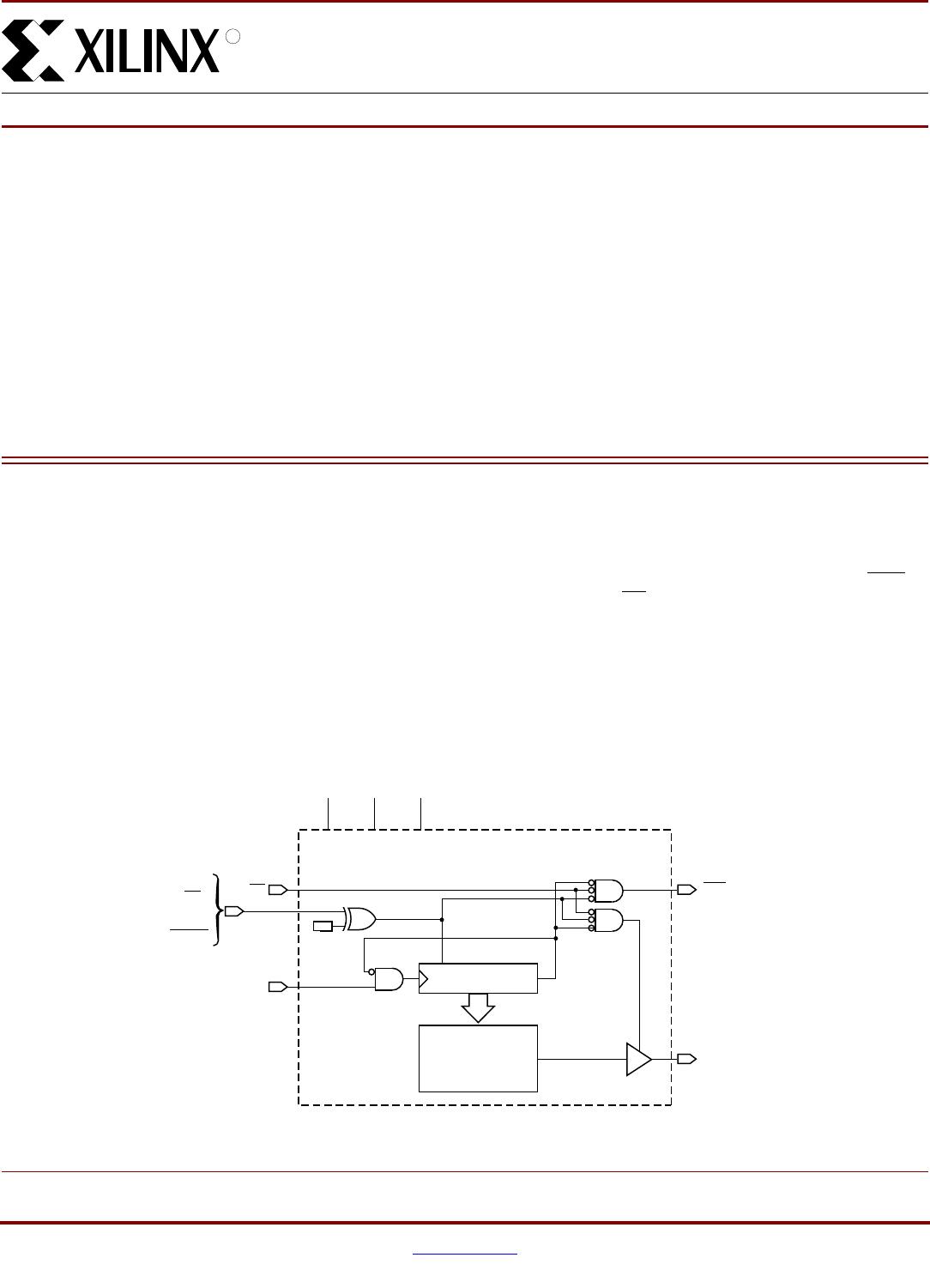
FPGA configuration bitstreams. See Figure 1 for a
simplified block diagram.
When the FPGA is in Master Serial mode, it generates a
configuration clock that drives the PROM. A short access
time after the rising clock edge, data appears on the PROM
DATA output pin that is connected to the FPGA D
IN
pin. The
FPGA generates the appropriate number of clock pulses to
complete the configuration. After configured, it disables the
PROM. When the FPGA is in Slave Serial mode, the PROM
and the FPGA must both be clocked by an incoming signal.
Multiple devices can be concatenated by using the CEO
output to drive the CE
input of the following device. The
clock inputs and the DATA outputs of all PROMs in this
chain are interconnected. All devices are compatible and
can be cascaded with other members of the family.
For device programming, either the Xilinx Alliance or
Foundation software compiles the FPGA design file into a
standard Hex format, which is then transferred to most
commercial PROM programmers.
<
B
L
XC1700E, XC1700EL, and XC1700L
Series Configuration PROMs
DS027 (v3.5) June 25, 2008
8
Product Specification
R
X-Ref Target - Figure 1
Figure 1: Simplified Block Diagram (Does Not Show Programming Circuit)
EPROM
Cell
Matrix
Address Counter
CE
DATA
OE
Output
CLK
V
CC
V
PP
GND
DS027_01_021500
TC
OE
RESET/
OE/
RESET
or
CEO
Product Obsolete or Under Obsolescence
XC1700E, XC1700EL, and XC1700L Series Configuration PROMs
DS027 (v3.5) June 25, 2008 www.xilinx.com
Product Specification 2
R
Pin Description
DATA
Data output is in a high-impedance state when either CE or
OE
are inactive. During programming, the DATA pin is I/O.
Note that OE
can be programmed to be either active High or
active Low.
CLK
Each rising edge on the CLK input increments the internal
address counter, if both CE
and OE are active.
RESET/OE
When High, this input holds the address counter reset and
puts the DATA output in a high-impedance state. The
polarity of this input pin is programmable as either
RESET/OE
or OE/RESET. To avoid confusion, this
document describes the pin as RESET/OE
, although the
opposite polarity is possible on all devices. When RESET is
active, the address counter is held at "0", and puts the DATA
output in a high-impedance state. The polarity of this input
is programmable. The default is active High RESET, but the
preferred option is active Low RESET
, because it can be
driven by the FPGAs INIT
pin.
The polarity of this pin is controlled in the programmer
interface. This input pin is easily inverted using the Xilinx
HW-130 Programmer. Third-party programmers have
different methods to invert this pin.
CE
When High, this pin disables the internal address counter,
puts the DATA output in a high-impedance state, and forces
the device into low-I
CC
standby mode.
CEO
Chip Enable output, to be connected to the CE input of the next
PROM in the daisy chain. This output is Low when the CE
and
OE
inputs are both active AND the internal address counter
has been incremented beyond its Terminal Count (TC) value.
In other words: when the PROM has been read, CEO
follows
CE
as long as OE is active. When OE goes inactive, CEO
stays High until the PROM is reset. Note that OE
can be
programmed to be either active High or active Low.
V
PP
Programming voltage. No overshoot above the specified
max voltage is permitted on this pin. For normal read
operation, this pin must be connected to V
CC
. Failure to do
so may lead to unpredictable, temperature-dependent
operation and severe problems in circuit debugging. Do not
leave V
PP
floating!
V
CC
and GND
Positive supply and ground pins.
PROM Pinouts
Pins not listed are "no connects."
"
Capacity
Pin Name
8-pin
PDIP
(PD8/
PDG8
)
SOIC
(SO8/
SOG8)
VOIC
(VO8/
VOG8)
20-pin
SOIC
(SO20)
20-pin
PLCC
(PC20/
PCG20)
44-pin
VQFP
(VQ44)
44-pin
PLCC
(PC44)
DATA 1 1 2 40 2
CLK 2 3 4 43 5
RESET/OE
(OE/RESET)
3861319
CE 4 10 8 15 21
GND 5 11 10 18, 41 24, 3
CEO 6 13 14 21 27
V
PP
718173541
V
CC
820203844
Devices Configuration Bits
XC1704L 4,194,304
XC1702L 2,097,152
XC1701/L 1,048,576
XC17512L 524,288
XC1736E 36,288
XC1765E/EL 65,536
XC17128E/EL 131,072
XC17256E/EL 262,144
Product Obsolete or Under Obsolescence
XC1700E, XC1700EL, and XC1700L Series Configuration PROMs
DS027 (v3.5) June 25, 2008 www.xilinx.com
Product Specification 3
R
Pinout Diagrams
6
5
4
3
2
1
44
43
42
41
40
39
38
37
36
35
34
33
32
31
30
29
18
19
20
21
22
23
24
25
26
27
28
7
8
9
10
11
12
13
14
15
16
17
PC44
Top View
NC
NC
NC
NC
NC
NC
NC
NC
NC
NC
NC
NC
RESET/OE
NC
CE
NC
NC
GND
NC
NC
CEO
NC
NC
CLK
NC
GND
DATA(D0)
NC
VCC
NC
NC
VPP
NC
DS027_05_090602
NC
NC
NC
NC
NC
NC
NC
NC
NC
NC
NC
PD8/PDG8
VO8/VOG8
SO8/SOG8
Top View
DS027_06_060705
VCC
VPP
CEO
GND
DATA(D0)
CLK
OE/RESET
CE
8
7
6
5
1
2
3
4
VQ44
Top View
NC
NC
NC
NC
NC
NC
NC
NC
NC
NC
NC
NC
RESET/OE
NC
CE
NC
NC
GND
NC
NC
CEO
NC
NC
CLK
NC
GND
DATA(D0)
NC
VCC
NC
NC
VPP
NC
DS027_07_090602
NC
NC
NC
NC
NC
NC
NC
NC
NC
NC
NC
1
2
3
4
5
6
7
8
9
10
11
44
43
42
41
40
39
38
37
36
35
34
33
32
31
30
29
28
27
26
25
24
23
12
13
14
15
16
17
18
19
20
21
22
PC20/PCG20
Top View
DS027_09_060705
3
2
1
20
19
18
17
16
15
14
9
10
11
12
13
4
5
6
7
8
NC
DATA(D0)
NC
VCC
NC
NC
VPP
NC
NC
CEO
NC
GND
NC
NC
NC
CLK
NC
OE/RESET
NC
CE
Product Obsolete or Under Obsolescence

XC17128EPC20C

Mfr. #:
Manufacturer:
Xilinx
Description:
Lifecycle:
New from this manufacturer.
Delivery:
DHL FedEx Ups TNT EMS
Payment:
T/T Paypal Visa MoneyGram Western Union