XC1700E, XC1700EL, and XC1700L Series Configuration PROMs
DS027 (v3.5) June 25, 2008 www.xilinx.com
Product Specification 7
XC1701, XC1736E, XC1765E, XC17128E and XC17256E
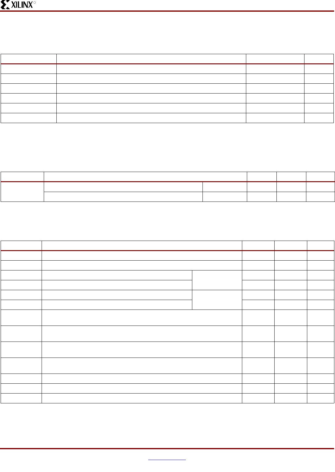
Absolute Maximum Ratings
Operating Conditions (5V Supply)
DC Characteristics Over Operating Condition
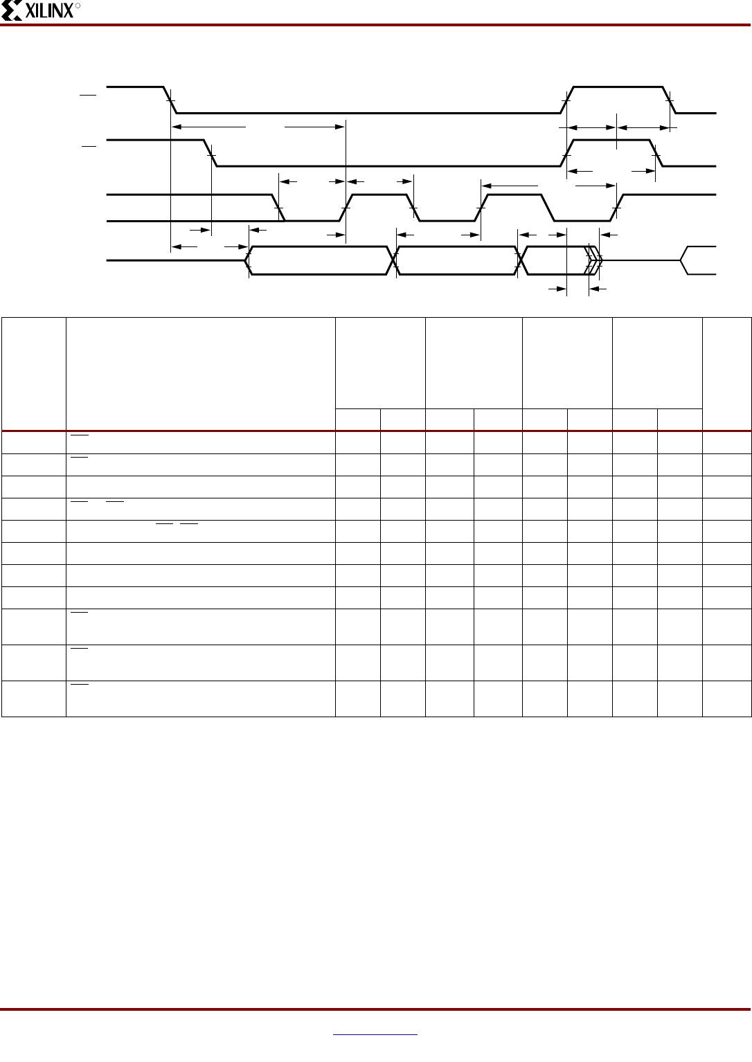
Symbol Description Conditions Units
V
CC
Supply voltage relative to GND –0.5 to +7.0 V
V
PP
Supply voltage relative to GND –0.5 to +12.5 V
V
IN
Input voltage relative to GND –0.5 to V
CC
+0.5 V
V
TS
Voltage applied to High-Z output –0.5 to V
CC
+0.5 V
T
STG
Storage temperature (ambient) –65 to +150 °C
T
J
Junction temperature +125 °C
Notes:
1. Stresses beyond those listed under Absolute Maximum Ratings may cause permanent damage to the device. These are stress ratings only,
and functional operation of the device at these or any other conditions beyond those listed under Operating Conditions is not implied.
Exposure to Absolute Maximum Ratings conditions for extended periods of time may affect device reliability.
Symbol Description Min Max Units
V
CC
(1)
Supply voltage relative to GND (T
A
= 0°C to +70°C) Commercial 4.750 5.25 V
Supply voltage relative to GND (T
A
= –40°C to +85°C) Industrial 4.50 5.50 V
Notes:
1. During normal read operation V
PP
must be connect to V
CC.
Symbol Description Min Max Units
V
IH
High-level input voltage 2 V
CC
V
V
IL
Low-level input voltage 0 0.8 V
V
OH
High-level output voltage (I
OH
= –4 mA) Commercial 3.86 – V
V
OL
Low-level output voltage (I
OL
= +4 mA) – 0.32 V
V
OH
High-level output voltage (I
OH
= –4 mA) Industrial 3.76 – V
V
OL
Low-level output voltage (I
OL
= +4 mA) – 0.37 V
I
CCA
Supply current, active mode at maximum frequency
(XC1736E, XC1765E, XC17128E, and XC17256E)
–10mA
I
CCA
Supply current, active mode at maximum frequency
(XC1701)
–20mA
I
CCS
Supply current, standby mode
(XC1736E, XC1765E, XC17128E, and XC17256E)
–50
(1)
μA
I
CCS
Supply current, standby mode
(XC1701)
–100
(1)
μA
I
L
Input or output leakage current –10 10 μA
C
IN
Input capacitance (V
IN
= GND, f = 1.0 MHz) – 10 pF
C
OUT
Output capacitance (V
IN
= GND, f = 1.0 MHz) – 10 pF
Notes:
1. I
CCS
standby current is specified for DATA pin that is pulled to V
CC
or GND.
Product Obsolete or Under Obsolescence