5
Functional Pin Description
UGATE (Pin 1 for SOIC-8, Pin 8 for QFN)
The UGATE pin is the upper gate drive output. Connect to
the gate of high-side power N-Channel MOSFET.
BOOT (Pin 2 for SOIC-8, Pin 1 for QFN)
BOOT is the floating bootstrap supply pin for the upper gate
drive. Connect the bootstrap capacitor between this pin and
the PHASE pin. The bootstrap capacitor provides the charge
to turn on the upper MOSFET. See the Bootstrap Diode and
Capacitor section under DESCRIPTION for guidance in
choosing the appropriate capacitor value.
PWM (Pin 3 for SOIC-8, Pin 2 for QFN)
The PWM signal is the control input for the driver. The PWM
signal can enter three distinct states during operation, see the
three-state PWM Input section under DESCRIPTION for further
details. Connect this pin to the PWM output of the controller.
GND (Pin 4 for SOIC-8, Pin 3 for QFN)
GND is the ground pin for the IC.
LGATE (Pin 5 for SOIC-8, Pin 4 for QFN)
LGATE is the lower gate drive output. Connect to gate of the
low-side power N-Channel MOSFET.
VCC (Pin 6 for SOIC-8, Pin 5 for QFN)
Connect the VCC pin to a +5V bias supply. Place a high
quality bypass capacitor from this pin to GND.
FCCM (Pin 7 for SOIC-8, Pin 6 for QFN)
The FCCM pin enables or disables Diode Emulation. When
FCCM is LOW, diode emulation is allowed. Otherwise,
continuous conduction mode is forced (FCCM= Forced
Continuous Conduction Mode). See the Diode Emulation
section under DESCRIPTION for more detail.
PHASE (Pin 8 for SOIC-8, Pin 7 for QFN)
Connect the PHASE pin to the source of the upper MOSFET
and the drain of the lower MOSFET. This pin provides a
return path for the upper gate driver.
Thermal Pad (in QFN only)
The PCB “thermal land” design for this exposed die pad
should include thermal vias that drop down and connect to
one or more buried copper plane(s). This combination of
vias for vertical heat escape and buried planes for heat
spreading allows the QFN to achieve its full thermal
potential. This pad should be grounded. Refer to TB389 for
design guidelines.
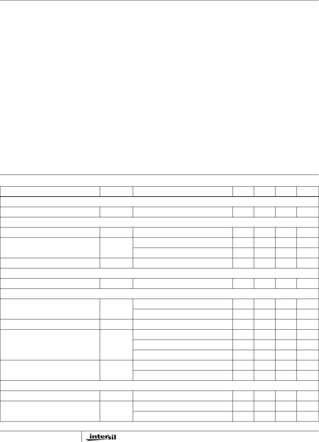
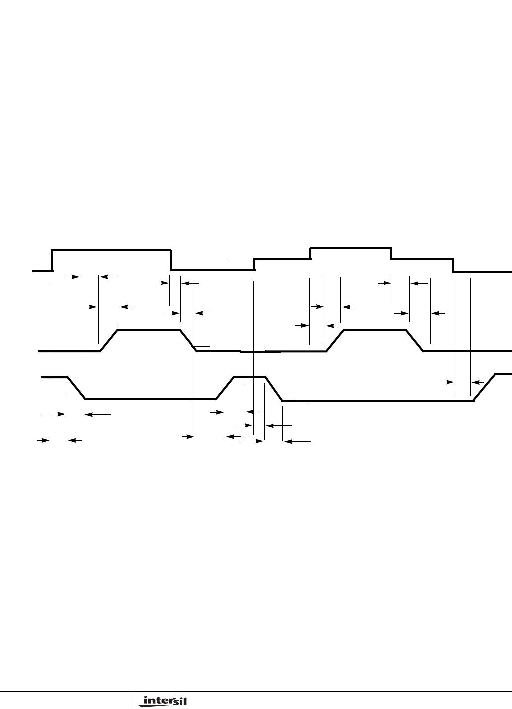
SWITCHING TIME
UGATE Rise Time t
RU
V
VCC
= 5V, 3nF Load - 8.0 - ns
LGATE Rise Time t
RL
V
VCC
= 5V, 3nF Load - 8.0 - ns
UGATE Fall Time t
FU
V
VCC
= 5V, 3nF Load - 8.0 - ns
LGATE Fall Time t
FL
V
VCC
= 5V, 3nF Load - 4.0 - ns
UGATE Turn-Off Propagation Delay t
PDLU
V
VCC
= 5V, Outputs Unloaded - 35 - ns
LGATE Turn-Off Propagation Delay t
PDLL
V
VCC
= 5V, Outputs Unloaded - 35 - ns
UGATE Turn-On Propagation Delay t
PDHU
V
VCC
= 5V, Outputs Unloaded - 20 - ns
LGATE Turn-On Propagation Delay t
PDHL
V
VCC
= 5V, Outputs Unloaded - 20 - ns
UG/LG Three-state Propagation Delay t
PTS
V
VCC
= 5V, Outputs Unloaded - 35 - ns
Minimum LG On TIME in DCM (Note 5) t
LGMIN
- 400 - ns
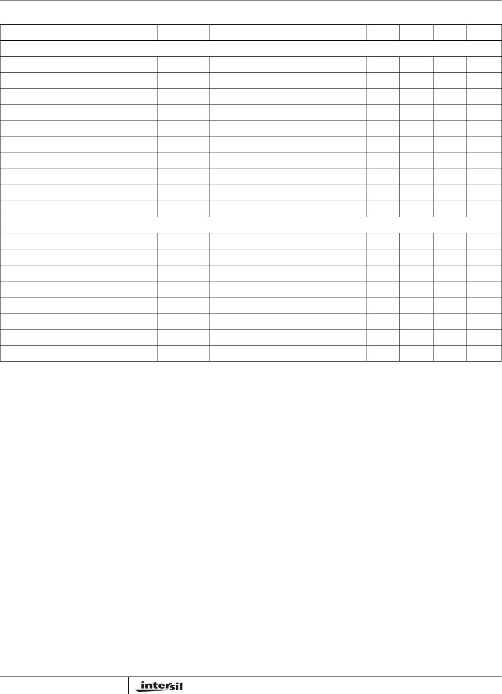
OUTPUT
Upper Drive Source Resistance R
U
250mA Source Current - 1 2.5 Ω
Upper Driver Source Current (Note 5) I
U
V
UGATE-PHASE
= 2.5V - 2.00 - A
Upper Drive Sink Resistance R
U
250mA Sink Current - 1 2.5 Ω
Upper Driver Sink Current (Note 5) I
U
V
UGATE-PHASE
= 2.5V - 2.00 - A
Lower Drive Source Resistance R
L
250mA Source Current - 1 2.5 Ω
Lower Driver Source Current (Note 5) I
L
V
LGATE
= 2.5V - 2.00 - A
Lower Drive Sink Resistance R
L
250mA Sink Current - 0.5 1.0 Ω
Lower Driver Sink Current (Note 5) I
L
V
LGATE
= 2.5V - 4.00 - A
Electrical Specifications Recommended Operating Conditions, Unless Otherwise Noted (Continued)
PARAMETER SYMBOL TEST CONDITIONS MIN TYP MAX UNITS
ISL6608