8
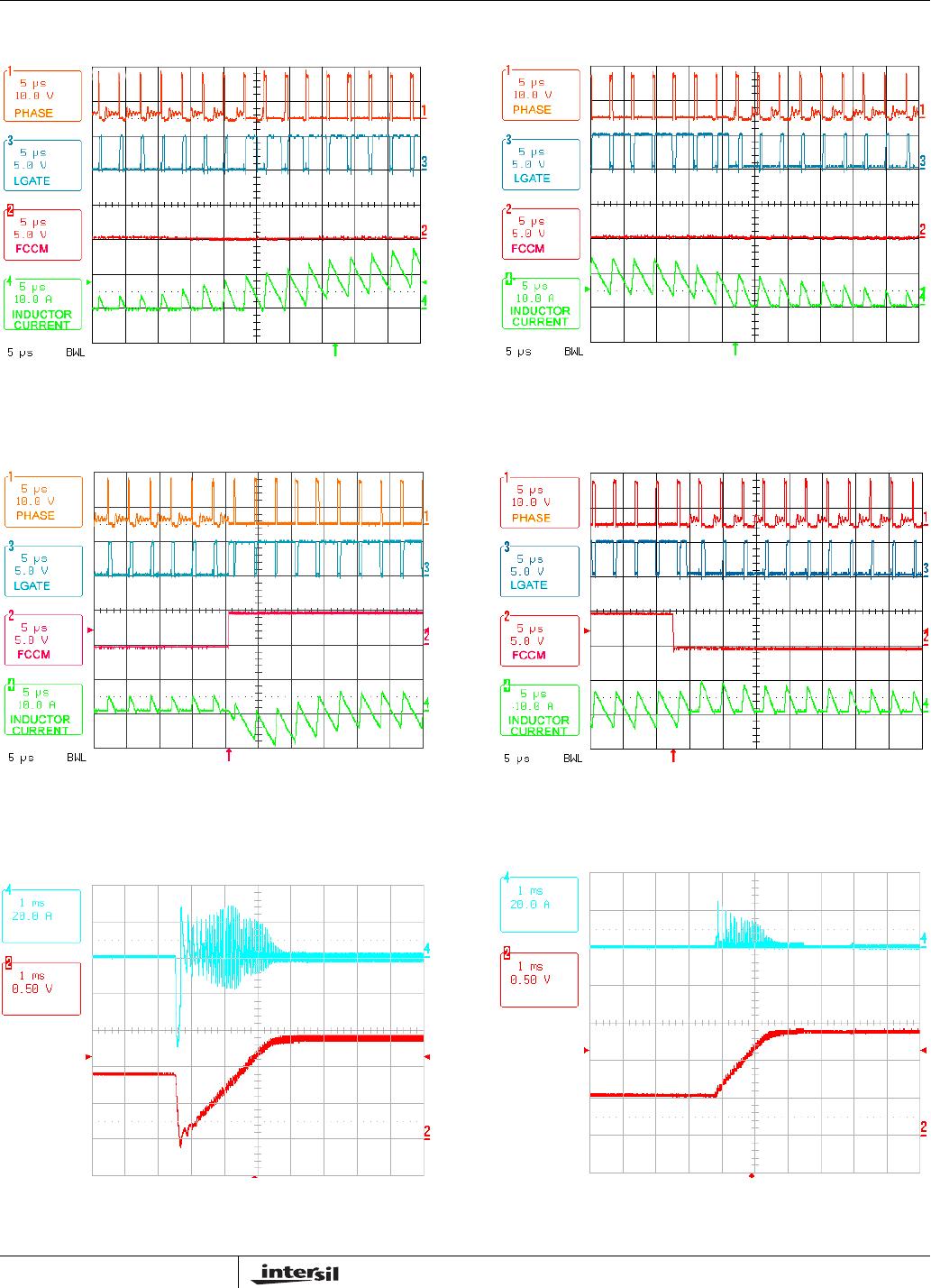
Diode Emulation
Diode emulation allows for higher converter efficiency under
light-load situations. With diode emulation active
(FCCM = LO), the ISL6608 will detect the zero current
crossing of the output inductor and turn off LGATE. This
ensures that discontinuous conduction mode (DCM) is
achieved. This prevents the low side MOSFET from sinking
current, and no negative spike at the output is generated
during pre-biased startup (See Figure 7 on page 7). The
LGATE has a minimum ON time of 400ns in DCM mode.
Diode emulation is asynchronous to the PWM signal.
Therefore, the ISL6608 responds to the FCCM input
immediately after it changes state. Refer to Figures 2 to 7 on
page 7 for details.
Intersil does not recommend Diode Emulation used with the
r
DS(ON)
of the freewheeling MOSFET current sensing
topology. The turn-OFF of the low side MOSFET forces the
forward current going through the body diode of the
MOSFET. If the current sampling circuit of the controller is
activated during the body diode conduction, a diode voltage
drop, instead of a much smaller MOSFET’s r
DS(ON)
voltage
drop, is sampled. This will falsely trigger the over current
protection function of the controller.
The ISL6608 works with DCR, upper MOSFET, or power
resistor current sensing topologies to start up from pre-
biased load with no problem.
Three-State PWM Input
A unique feature of the ISL6608 and other Intersil drivers is
the addition of a shutdown window to the PWM input. If the
PWM signal enters and remains within the shutdown window
for a set holdoff time (typically 160ns), the output drivers are
disabled and both MOSFET gates are pulled and held low.
The shutdown state is removed when the PWM signal
moves outside the shutdown window. Otherwise, the PWM
rising and falling thresholds outlined in the ELECTRICAL
SPECIFICATIONS determine when the lower and upper
gates are enabled.
Adaptive Shoot-Through Protection
Both drivers incorporate adaptive shoot-through protection
to prevent upper and lower MOSFETs from conducting
simultaneously and shorting the input supply. This is
accomplished by ensuring the falling gate has turned off one
MOSFET before the other is allowed to turn on.
During turn-off of the lower MOSFET, the LGATE voltage is
monitored until it reaches a 1V threshold, at which time the
UGATE is released to rise. Adaptive shoot-through circuitry
monitors the upper MOSFET gate-to-source voltage during
UGATE turn-off. Once the upper MOSFET gate-to-source
voltage has dropped below a threshold of 1V, the LGATE is
allowed to rise.
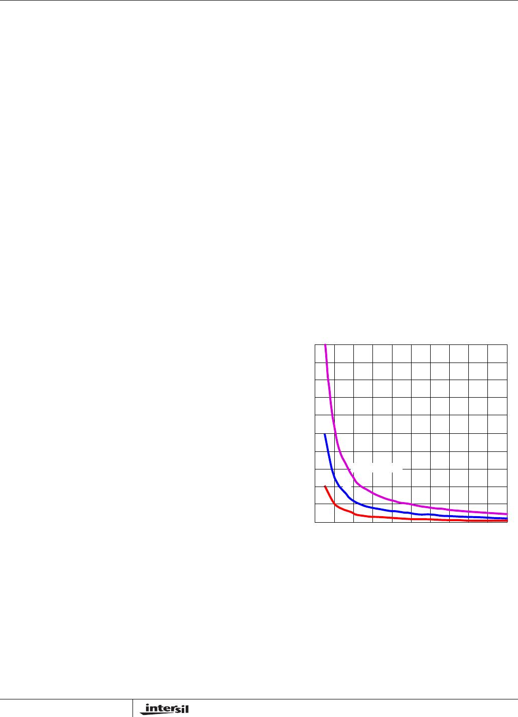
Internal Bootstrap Diode
This driver features an internal bootstrap Schottky diode.
Simply adding an external capacitor across the BOOT and
PHASE pins completes the bootstrap circuit. The bootstrap
capacitor must have a maximum voltage rating above VCC +
5V and its capacitance value can be chosen from the
following equation:
where Q
G1
is the amount of gate charge per upper MOSFET
at V
GS1
gate-source voltage and N
Q1
is the number of
control MOSFETs. The ∆V
BOOT
term is defined as the
allowable droop in the rail of the upper drive. The previous
relationship is illustrated in Figure 8.
As an example, suppose an upper MOSFET has a gate
charge, Q
GATE
, of 65nC at 5V and also assume the droop in
the drive voltage over a PWM cycle is 200mV. One will find
that a bootstrap capacitance of at least 0.125µF is required.
The next larger standard value capacitance is 0.15µF. A
good quality ceramic capacitor is recommended.
C
BOOT
Q
GATE
∆V
BOOT
------------------------
≥
Q
GATE
Q
G1
VCC•
V
GS1
-------------------------------
N
Q1
•=
FIGURE 8. BOOTSTRAP CAPACITANCE vs BOOT RIPPLE
VOLTAGE
20nC
∆V
BOOT_CAP
(V)
C
BOOT_CAP
(µF)
2.0
1.6
1.4
1.0
0.8
0.6
0.4
0.2
0.0
0.30.0 0.1 0.2 0.4 0.5 0.6 0.90.7 0.8 1.0
Q
GATE
= 100nC
1.2
1.8
5
0
n
C
ISL6608