32MB, 64MB, 128MB (x72, SR)
168-PIN SDRAM UDIMM
32, 64, 128MB x 64 SDRAM DIMM Micron Technology, Inc., reserves the right to change products or specifications without notice.
SD5C4_8_16x72AG.fm - Rev. C 6/04 EN
12 ©2004 Micron Technology, Inc. All rights reserved.
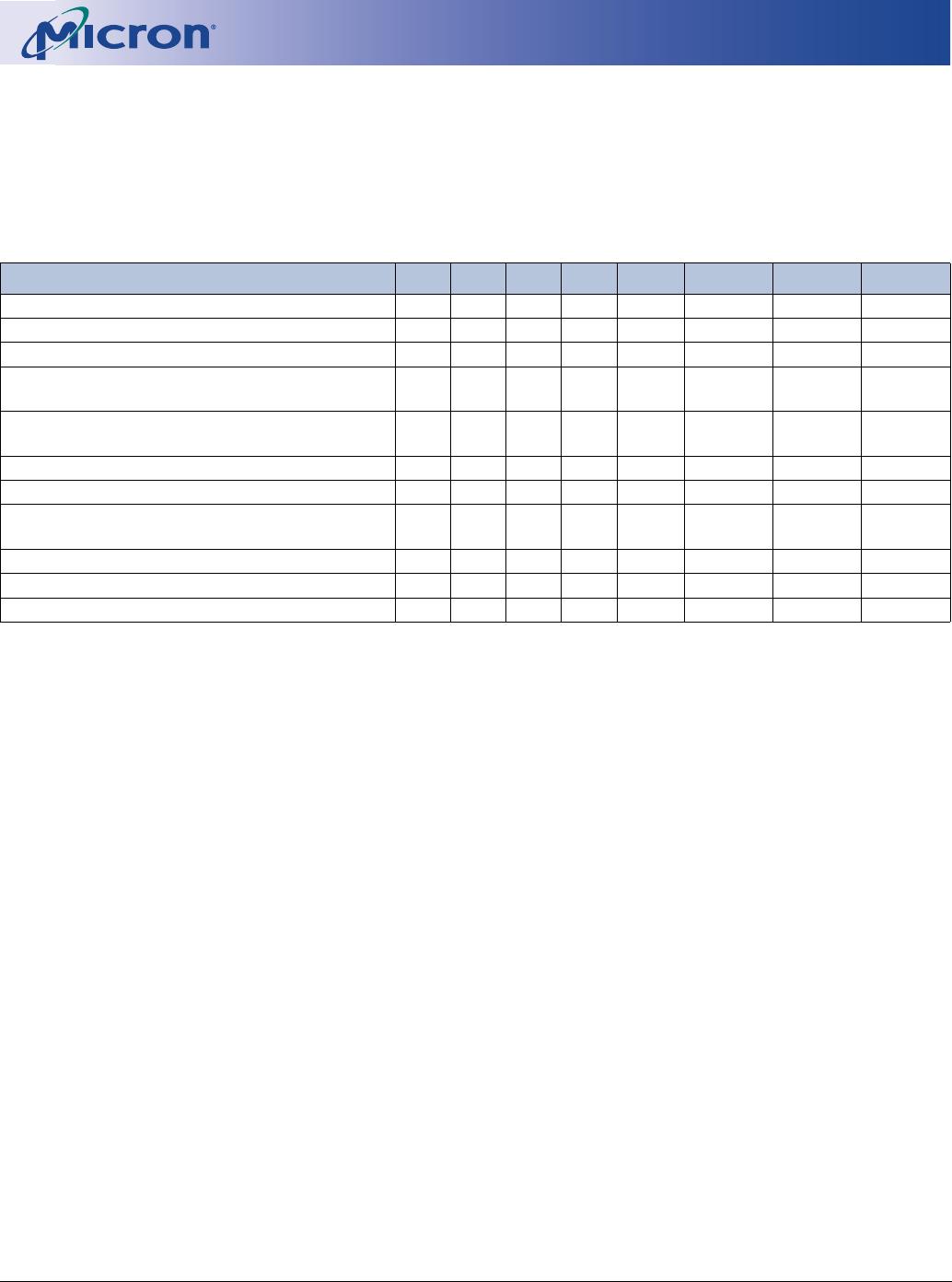
Absolute Maximum Ratings
Stresses greater than those listed may cause perma-
nent damage to the device. This is a stress rating only,
and functional operation of the device at these or any
other conditions above those indicated in the opera-
tional sections of this specification is not implied.
Exposure to absolute maximum rating conditions for
extended periods may affect reliability.
Voltage on V
DD, VDDQ Supply
Relative to V
SS . . . . . . . . . . . . . . . . . . . .-1V to +4.6V
Voltage on Inputs, NC or I/O Pins
Relative to V
SS . . . . . . . . . . . . . . . . . . . .-1V to +4.6V
Operating Temperature
T
OPR
(Commercial - ambient) . . . . . .0°C to +65°C
T
OPR
(Industrial - ambient). . . . . . .-40°C to +85°C
Storage Temperature (plastic) . . . . . .-55°C to +150°C
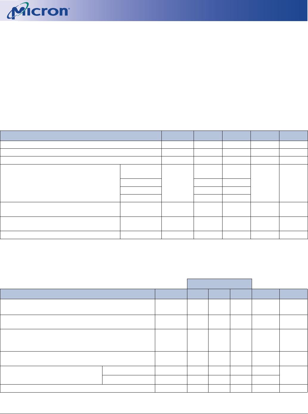
Table 10: DC Electrical Characteristics and Operating Conditions
Notes: 1, 5, 6; notes appear following the parameter tables; VDD, VDDQ = +3.3V ±0.3V
PARAMETER/CONDITION SYMBOL MIN MAX UNITS NOTES
SUPPLY VOLTAGE
V
DD, VDDQ3 3.6 V
INPUT HIGH VOLTAGE: Logic 1; All inputs
V
IH 2VDD + 0.3 V22
INPUT LOW VOLTAGE: Logic 0; All inputs
V
IL -0.3 0.8 V 22
INPUT LEAKAGE CURRENT: Any input 0V ≤ V
IN
≤ V
DD (All other pins not under
test = 0V)
Command/
Address, CKE
I
I
-25 25
µA 33
CK, S0#
-15 15
CK2, S2#
-10 10
DQMB
-5 5
OUTPUT LEAKAGE CURRENT: DQs are disabled;
0V ≤ V
OUT ≤ VDDQ
DQ
IOZ -5 5 µA 33
OUTPUT LEVELS: Output High Voltage (I
OUT = -
4mA)
V
OH 2.4 – V
Output Low Voltage (IOUT = 4mA)
V
OL –0.4V
Table 11: IDD Specifications and Conditions – 32MB
Notes: 1, 5, 6, 11, 13; notes appear following the parameter tables; VDD, VDDQ = +3.3V ±0.3V; DRAM components only
MAX
PARAMETER/CONDITION SYMBOL -13E -133 -10E UNITS NOTES
OPERATING CURRENT: Active Mode; Burst = 2; READ or
WRITE;
t
RC =
t
RC (MIN)
I
DD1 625 575 475 mA 3, 18, 19,
29
STANDBY CURRENT: Power-Down Mode; All device banks
idle; CKE = LOW
I
DD2 10 10 10 mA 29
STANDBY CURRENT: Active Mode; CKE = HIGH; CS# = HIGH;
All device banks active after
t
RCD met; No accesses in
progress
I
DD3 225 225 175 mA 3, 12, 19,
29
OPERATING CURRENT: Burst Mode; Continuous burst; READ
or WRITE; All device banks active
I
DD4 750 700 600 mA 3, 18, 19,
29
AUTO REFRESH CURRENT
CS# = HIGH; CKE = HIGH
t
RFC =
t
RFC (MIN)
I
DD5 1,150 1,050 950 mA 3, 12, 18,
19, 29, 30
t
RFC = 15.62µs
I
DD6 15 15 15 mA
SELF REFRESH CURRENT: CKE ≤ 0.2V
I
DD7 555mA 4