32MB, 64MB, 128MB (x72, SR)
168-PIN SDRAM UDIMM
32, 64, 128MB x 64 SDRAM DIMM Micron Technology, Inc., reserves the right to change products or specifications without notice.
SD5C4_8_16x72AG.fm - Rev. C 6/04 EN
13 ©2004 Micron Technology, Inc. All rights reserved.
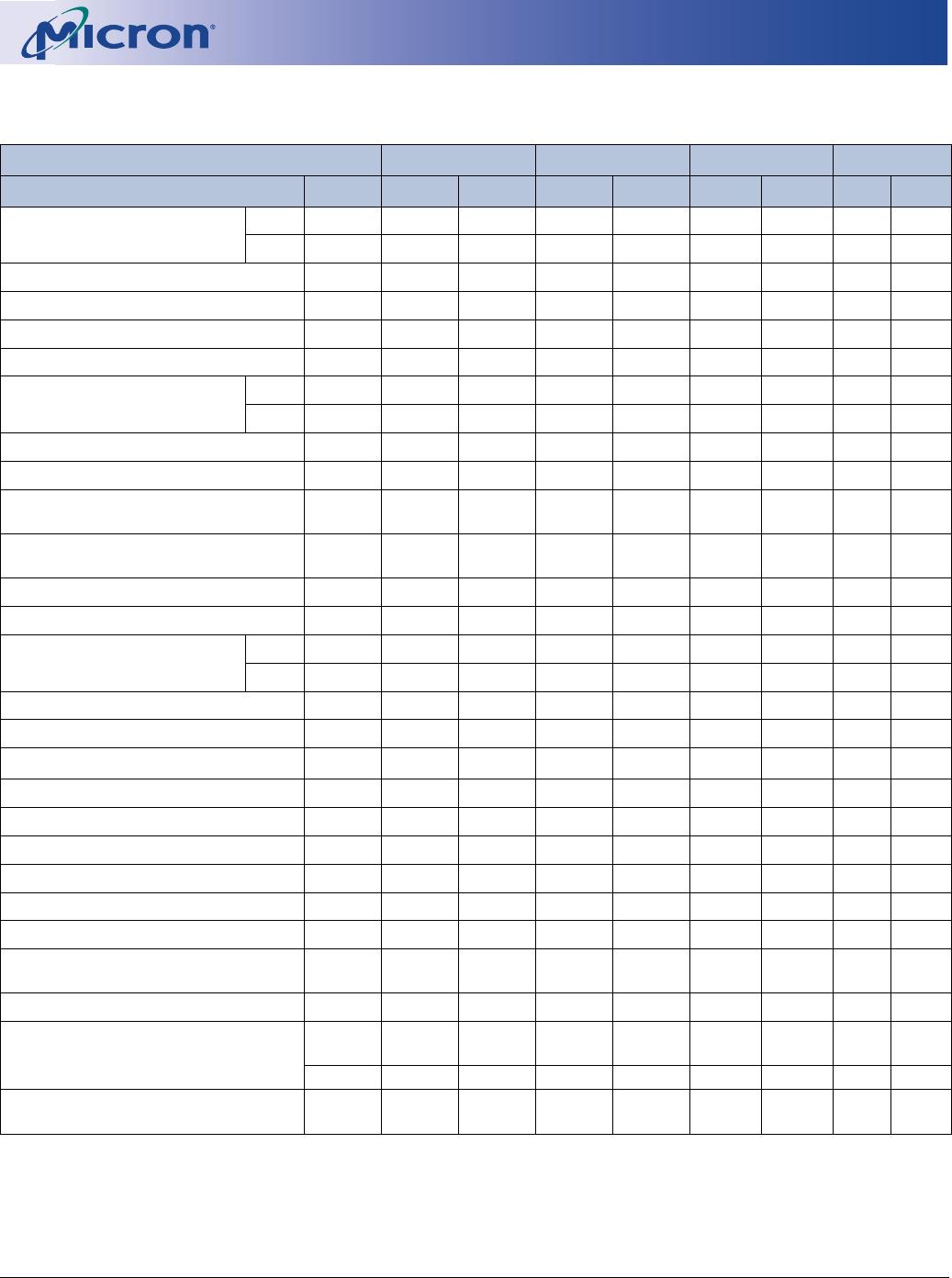
Table 12: IDD Specifications and Conditions – 64MB
Notes: 1, 5, 6, 11, 13; notes appear following the parameter tables; VDD, VDDQ = +3.3V ±0.3V; DRAM components only
MAX
PARAMETER/CONDITION SYMBOL -13E -133 -10E UNITS NOTES
OPERATING CURRENT: Active Mode; Burst = 2; READ or
WRITE;
t
RC =
t
RC (MIN)
I
DD1 800 750 700 mA 3, 18, 19,
29
STANDBY CURRENT: Power-Down Mode; All device banks
idle; CKE = LOW
I
DD2 10 10 10 mA 29
STANDBY CURRENT: Active Mode; CKE = HIGH; CS# = HIGH;
All device banks active after
t
RCD met; No accesses in
progress
I
DD3 250 250 200 mA 3, 12, 19,
29
OPERATING CURRENT: Burst Mode; Continuous burst; READ
or WRITE; All device banks active
I
DD4 825 750 700 mA 3, 18, 19,
29
AUTO REFRESH CURRENT
CS# = HIGH; CKE = HIGH
t
RFC =
t
RFC (MIN)
IDD5 1,650 1,550 1,350 mA 3, 12, 18,
19, 29, 30
t
RFC = 15.62µs
I
DD6 15 15 15 mA
SELF REFRESH CURRENT: CKE 0.2V
I
DD7 10 10 10 mA 4
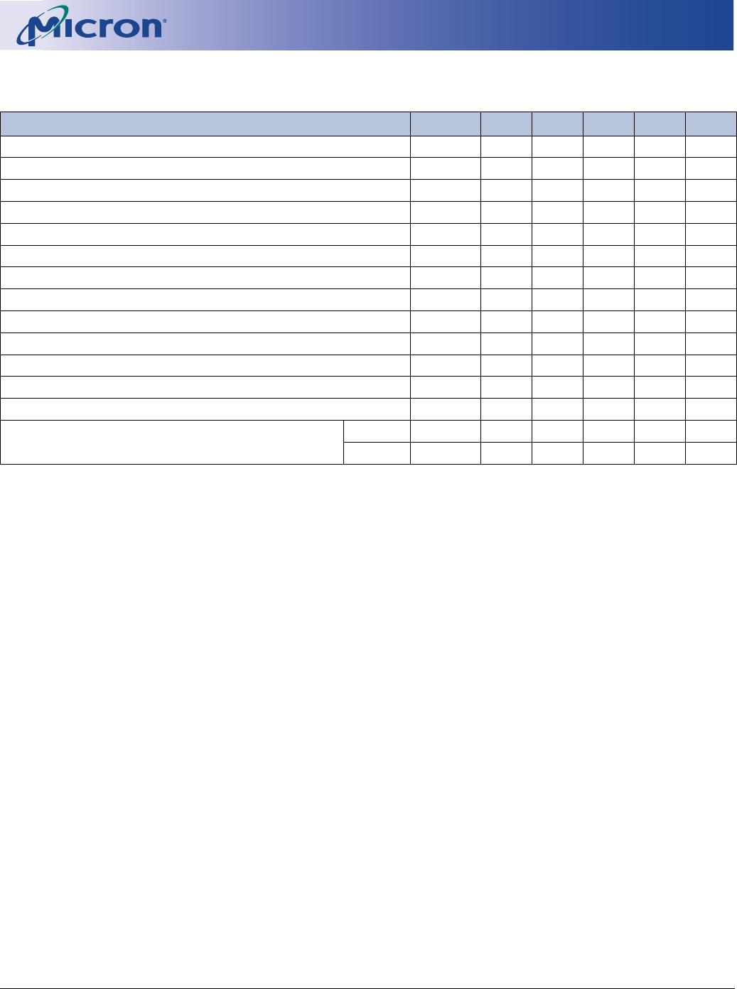
Table 13: IDD Specifications and Conditions – 128MB
Notes: 1, 5, 6, 11, 13; notes appear following the parameter tables; VDD, VDDQ = +3.3V ±0.3V; DRAM components only
MAX
PARAMETER/CONDITION SYMBOL -13E -133 -10E UNITS NOTES
OPERATING CURRENT: Active Mode; Burst = 2; READ or
WRITE;
t
RC =
t
RC (MIN)
IDD1 625 625 625 mA 3, 18, 19,
29
STANDBY CURRENT: Power-Down Mode; All device banks
idle; CKE = LOW
IDD2 10 10 10 mA 29
STANDBY CURRENT: Active Mode; CKE = HIGH; CS# = HIGH;
All device banks active after
t
RCD met; No accesses in
progress
I
DD3 200 200 200 mA 3, 12, 19,
29
OPERATING CURRENT: Burst Mode; Continuous burst; READ
or WRITE; All device banks active
I
DD4 675 675 675 mA 3, 18, 19,
29
AUTO REFRESH CURRENT
CS# = HIGH; CKE = HIGH
t
RFC =
t
RFC (MIN)
IDD5 1,425 1,350 1,350 mA 3, 12, 18,
19, 29, 30
t
RFC = 7.81µs
I
DD6 17.5 17.5 17.5 mA
SELF REFRESH CURRENT: CKE 0.2V
I
DD7 12.5 12.5 12.5 mA 4
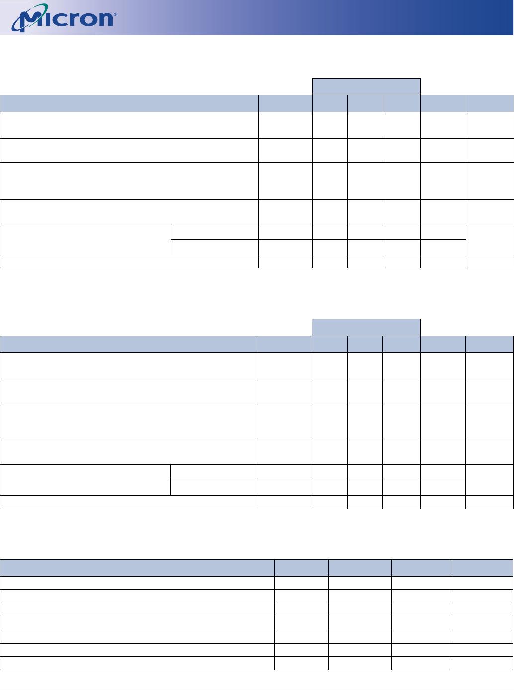
Table 14: Capacitance
Notes 1, 2; notes appear following parameter table
PARAMETER SYMBOL MIN MAX UNITS
Input Capacitance: Address and Command, CKE
C
I1 12.5 19 pF
Input Capacitance: S0#
C
I2
a
7.5 11.4 pF
Input Capacitance: S2#
CI2
b
57.6pF
Input Capacitance: CK0
C
I3
a
14.1 17.1 pF
Input Capacitance: CK2
C
I3
b
18.6 20.6 pF
Input Capacitance: DQMB
C
I4 2.5 3.8 pF
Inuput/Output Capacitance: DQ
C
IO 46pF
32MB, 64MB, 128MB (x72, SR)
168-PIN SDRAM UDIMM
32, 64, 128MB x 64 SDRAM DIMM Micron Technology, Inc., reserves the right to change products or specifications without notice.
SD5C4_8_16x72AG.fm - Rev. C 6/04 EN
14 ©2004 Micron Technology, Inc. All rights reserved.
Table 15: Electrical Characteristics and Recommended AC Operating Conditions
Notes: 5, 6, 8, 9, 11, 31; notes appear following the parameter tables; VDD, VDDQ = +3.3V ±0.3V
AC CHARACTERISTICS -13E -133 -10E
PARAMETER
SYMBOL
MIN MAX MIN MAX MIN MAX
UNITS NOTES
Access time from CLK
(pos. edge)
CL = 3
t
AC(3)
5.4 5.4 6 ns 27
CL = 2
t
AC(2)
5.4 6 6 ns
Address hold time
t
AH
0.8 0.8 1 ns
Address setup time
t
AS
1.5 1.5 2 ns
CLK high-level width
t
CH
2.5 2.5 3 ns
CLK low-level width
t
CL
2.5 2.5 3 ns
Clock cycle time CL = 3
t
CK(3)
77.58ns23
CL = 2
t
CK(2)
7.5 10 10 ns 23
CKE hold time
t
CKH
0.8 0.8 1 ns
CKE setup time
t
CKS
1.5 1.5 2 ns
CS#, RAS#, CAS#, WE#, DQM hold
time
t
CMH
0.8 0.8 1 ns
CS#, RAS#, CAS#, WE#, DQM setup
time
t
CMS
1.5 1.5 2 ns
Data-in hold time
t
DH
0.8 0.8 1 ns
Data-in setup time
t
DS
1.5 1.5 2 ns
Data-out high-impedance
time
CL = 3
t
HZ(3)
5.4 5.4 6 ns 10
CL = 2
t
HZ(2)
5.4 6 6 ns 10
Data-out low-impedance time
t
LZ
111ns
Data-out hold time (load)
t
OH
333ns
Data-out hold time (no load)
t
OH
N
1.8 1.8 1.8 ns 28
ACTIVE to PRECHARGEcommand
t
RAS
37 120,000 44 120,000 50 120,000 ns 32
ACTIVE to ACTIVE command period
t
RC
60 66 70 ns
ACTIVE to READ or WRITE delay
t
RCD
15 20 20 ns
Refresh period (8,192 rows)
t
REF
64 64 64 ms
AUTO REFRESH period
t
RFC
66 66 70 ns
PRECHARGE command period
t
RP
15 20 20 ns
ACTIVE bank a to ACTIVE bank b
command
t
RRD
14 15 20 ns
Transition time
t
T
0.3 1.2 0.3 1.2 0.3 1.2 ns 7
WRITE recovery time
t
WR
1 CLK +
7ns
1 CLK +
7.5ns
1 CLK +
7ns
ns 24
14 15 15 ns 25
Exit SELF REFRESH to ACTIVE
command
t
XSR
67 75 80 ns 20
32MB, 64MB, 128MB (x72, SR)
168-PIN SDRAM UDIMM
32, 64, 128MB x 64 SDRAM DIMM Micron Technology, Inc., reserves the right to change products or specifications without notice.
SD5C4_8_16x72AG.fm - Rev. C 6/04 EN
15 ©2004 Micron Technology, Inc. All rights reserved.
Table 16: AC Functional Characteristics
Notes: 5, 6, 8, 9, 11, 31; notes appear following the parameter tables
PARAMETER SYMBOL -13E -133 -10E UNITS NOTES
READ/WRITE command to READ/WRITE command
t
CCD
111
t
CK
17
CKE to clock disable or power-down entry mode
t
CKED
111
t
CK
14
CKE to clock enable or power-down exit setup mode
t
PED
111
t
CK
14
DQM to input data delay
t
DQD
000
t
CK
17
DQM to data mask during WRITEs
t
DQM
000
t
CK
17
DQM to data high-impedance during READs
t
DQZ
222
t
CK
17
WRITE command to input data delay
t
DWD
000
t
CK
17
Data-in to ACTIVE command
t
DAL
454
t
CK
15, 21
Data-into PRECHARGE command
t
DPL
222
t
CK
16, 21
Last data-in to burst STOP command
t
BDL
111
t
CK
17
Last data-in to new READ/WRITE command
t
CDL
111
t
CK
17
Last data-in to PRECHARGE command
t
RDL
222
t
CK
16, 21
LOAD MODE REGISTER command to ACTIVE or REFRESH command
t
MRD
222
t
CK
26
Data-out to high-impedance from PRECHARGE
command
CL =3
t
ROH(3)
333
t
CK
17
CL = 2
t
ROH(2)
222
t
CK
17

MT5LSDT872AG-133G1

Mfr. #:
Manufacturer:
Micron
Description:
MODULE SDRAM 64MB 168UDIMM
Lifecycle:
New from this manufacturer.
Delivery:
DHL FedEx Ups TNT EMS
Payment:
T/T Paypal Visa MoneyGram Western Union