32MB, 64MB, 128MB (x72, SR)
168-PIN SDRAM UDIMM
32, 64, 128MB x 64 SDRAM DIMM Micron Technology, Inc., reserves the right to change products or specifications without notice.
SD5C4_8_16x72AG.fm - Rev. C 6/04 EN
19 ©2004 Micron Technology, Inc. All rights reserved.
NOTE:
1. To avoid spurious START and STOP conditions, a minimum delay is placed between SCL = 1 and the falling or rising
edge of SDA.
2. This parameter is sampled.
3. For a reSTART condition, or following a WRITE cycle.
4. The SPD EEPROM WRITE cycle time (
t
WRC) is the time from a valid stop condition of a write sequence to the end of
the EEPROM internal erase/program cycle. During the WRITE cycle, the EEPROM bus interface circuit is disabled, SDA
remains HIGH due to pull-up resistor, and the EEPROM does not respond to its slave address.
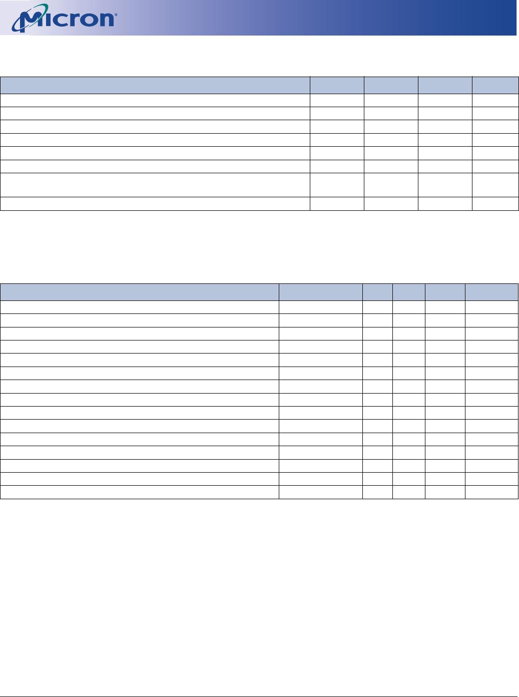
Table 19: Serial Presence-Detect EEPROM DC Operating Conditions
All voltages referenced to VSS; VDDSPD = +2.3V to +3.6V
PARAMETER/CONDITION SYMBOL MIN MAX UNITS
SUPPLY VOLTAGE
V
DD 33.6V
INPUT HIGH VOLTAGE: Logic 1; All inputs
V
IH VDD x 0.7 VDD + 0.5 V
INPUT LOW VOLTAGE: Logic 0; All inputs
V
IL -1 VDD x 0.3 V
OUTPUT LOW VOLTAGE: I
OUTL = 3mA
V
OL –0.4V
INPUT LEAKAGE CURRENT: V
IN = GND to VDD
ILI –10µA
OUTPUT LEAKAGE CURRENT: V
OUT = GND to VDD
ILO –10µA
STANDBY CURRENT: SCL = SDA = V
DD - 0.3V;
All other inputs = GND or 3.3V ±10%
I
SB –30µA
POWER SUPPLY CURRENT: SCL clock frequency = 100 KHz
I
DD –2mA
Table 20: Serial Presence-Detect EEPROM AC Operating Conditions
All voltages referenced to VSS; VDDSPD = +2.3V to +3.6V
PARAMETER/CONDITION SYMBOL MIN MAX UNITS NOTES
SCL LOW to SDA data-out valid
t
AA 0.2 0.9 µs 1
Time the bus must be free before a new transition can start
t
BUF 1.3 µs
Data-out hold time
t
DH 200 ns
SDA and SCL fall time
t
F 300 ns 2
Data-in hold time
t
HD:DAT 0 µs
Start condition hold time
t
HD:STA 0.6 µs
Clock HIGH period
t
HIGH 0.6 µs
Noise suppression time constant at SCL, SDA inputs
t
I50ns
Clock LOW period
t
LOW 1.3 µs
SDA and SCL rise time
t
R0.3µs2
SCL clock frequency
f
SCL 400 KHz
Data-in setup time
t
SU:DAT 100 ns
Start condition setup time
t
SU:STA 0.6 µs 3
Stop condition setup time
t
SU:STO 0.6 µs
WRITE cycle time
t
WRC 10 ms 4
32MB, 64MB, 128MB (x72, SR)
168-PIN SDRAM UDIMM
32, 64, 128MB x 64 SDRAM DIMM Micron Technology, Inc., reserves the right to change products or specifications without notice.
SD5C4_8_16x72AG.fm - Rev. C 6/04 EN
20 ©2004 Micron Technology, Inc. All rights reserved.
Table 21: Serial Presence-Detect Matrix
“1”/”0”: Serial Data, “driven to HIGH”/”driven to LOW.
BYTE DESCRIPTION
ENTRY
(VERSION)
MT5LSDT472A MT5LSDT872A(I) MT5LSDT1672A(I)
0
Number of Bytes Used By Micron
128 80 80 80
1
Total Number of Spd Memory Bytes
256 08 08 08
2
Memory Type
SDRAM 04 04 04
3
Number of Row Addresses
12 or 13 0C 0C 0D
4
Number of Column Addresses
8 or 9 08 09 09
5
Number of Banks
10101 01
6
Module Data Width
72 48 48 48
7
Module Data Width (Continued)
00000 00
8
Module Voltage Interface Levels
LVTTL 01 01 01
9
SDRAM Cycle Time,
t
CK
(CAS Latency = 3)
7ns (-13E)
7.5ns (-133)
8ns (-10E)
70
75
80
70
75
80
70
75
80
10
SDRAM Access from Clock,
t
AC
(CAS Latency = 3)
5.4ns (-13E/-133)
6ns (-10E)
54
60
54
60
54
60
11
Module Configuration Type
ECC 02 02 02
12
Refresh Rate/Type
(80) 15.6µs/SELF
(82) 7.81µs/SELF
80 80 82
13
SDRAM Width (Primary SDRAM)
16 10 10 10
14
Error-checking SDRAM Data Width
16 10 10 10
15
Minimum Clock Delay,
t
CCD
10101 01
16
Burst Lengths Supported
1, 2, 4, 8, PAGE 8F 8F 8F
17
Number of Internal Banks
on SDRAM Device
40404 04
18
CAS Latencies Supported
2, 3 06 06 06
19
CS Latency
00101 01
20
WE Latency
00101 01
21
SDRAM Module Attributes
UNBUFFERED 00 00 00
22
SDRAM Device Attributes: General
0E 0E 0E 0E
23
SDRAM Cycle Time,
t
CK
(CAS Latency = 2)
7.5ns (-13E)
10ns (-133/-10E)
75
A0
75
A0
75
A0
24
SDRAM Access from Clock,
t
AC
(CAS Latency = 2)
5.4ns (-13E)
6ns (-133/-10E)
54
60
54
60
54
60
25
SDRAM Cycle Time,
t
CK
(CAS Latency = 1)
–0000 00
26
SDRAM Access from Clock,
t
AC
(CAS Latency = 1)
–0000 00
27
Minimum Row Precharge Time,
t
RP
15ns (-13E)
20ns (-133/-10E)
0F
14
0F
14
0F
14
28
Minimum Row Active to Row Active,
t
RRD
14ns (-13E)
15ns (-133)
20ns (-10E)
0E
0F
14
0E
0F
14
0E
0F
14
29
Minimum RAS# to CAS# Delay,
t
RCD
15ns (-13E)
20ns (-133/-10E)
0F
14
0F
14
0F
14
32MB, 64MB, 128MB (x72, SR)
168-PIN SDRAM UDIMM
32, 64, 128MB x 64 SDRAM DIMM Micron Technology, Inc., reserves the right to change products or specifications without notice.
SD5C4_8_16x72AG.fm - Rev. C 6/04 EN
21 ©2004 Micron Technology, Inc. All rights reserved.
NOTE:
1. The value of
t
RAS used for the -13E part is calculated from
t
RC -
t
RP. Actual device specification value is 37ns.
30
Minimum RAS# Pulse Width,
t
RAS
(Note 1)
45ns (-13E)
44ns (-133)
50ns (-10E)
2D
2C
32
2D
2C
32
2D
2C
32
31
Module Rank Density
32MB, 64MB, or
128MB
08 10 20
32
Command and Address Setup Time
1.5ns (-13E/-133)
2ns (-10E)
15
20
15
20
15
20
33
Command and Address Hold Time
0.8ns (-13E/-133)
1ns (-10E)
08
10
08
10
08
10
34
Data Signal Input Setup Time
1.5ns (-13E/-133)
2ns (-10E)
15
20
15
20
15
20
35
Data Signal Input Hold Time
0.8ns (-13E/-133)
1ns (-10E)
08
10
08
10
08
10
36-40
Reserved
00 00 00
41
Device Minimum Active/Auto-refresh Time,
t
RC
60ns (-13E)
66ns (-133)
70ns (10E)
3C
42
46
3C
42
46
3C
42
46
42-61
Reserved
00 00 00
62
SPD Revision
2.0 02 20 20
63
Checksum for Bytes 0-62
-13E
-133
-10E
9C
E8
34
A5
F1
3D
B8
04
50
64
Manufacturer’s JEDEC ID Code
MICRON 2C 2C 2C
65-71
Manufacturer’s JEDEC ID Code (Continued)
FF FF FF
72
Manufacturing Location
1–12 01–0C 01–0C 01–0C
73-90
Module Part Number (ASCII)
Variable Data Variable Data Variable Data
91
PCB Identification Code
1-9 01-09 01-09 01-09
92
Identification Code (Continued)
00000 00
93
Year of Manufacture in BCD
Variable Data Variable Data Variable Data
94
Week of Manufacture in BCD
Variable Data Variable Data Variable Data
95-98
Module Serial Number
Variable Data Variable Data Variable Data
99-125
Manufacturer-Specific Data (RSVD)
Variable Data Variable Data Variable Data
126
System Frequency
100/133 MHz 64 64 64
127
SDRAM Component And Clock Detail
AF AF AF
Table 21: Serial Presence-Detect Matrix
“1”/”0”: Serial Data, “driven to HIGH”/”driven to LOW.
BYTE DESCRIPTION
ENTRY
(VERSION)
MT5LSDT472A MT5LSDT872A(I) MT5LSDT1672A(I)

MT5LSDT872AG-133G1

Mfr. #:
Manufacturer:
Micron
Description:
MODULE SDRAM 64MB 168UDIMM
Lifecycle:
New from this manufacturer.
Delivery:
DHL FedEx Ups TNT EMS
Payment:
T/T Paypal Visa MoneyGram Western Union