© 2006 Microchip Technology Inc. DS21204E-page 1
25AA040/25LC040/25C040
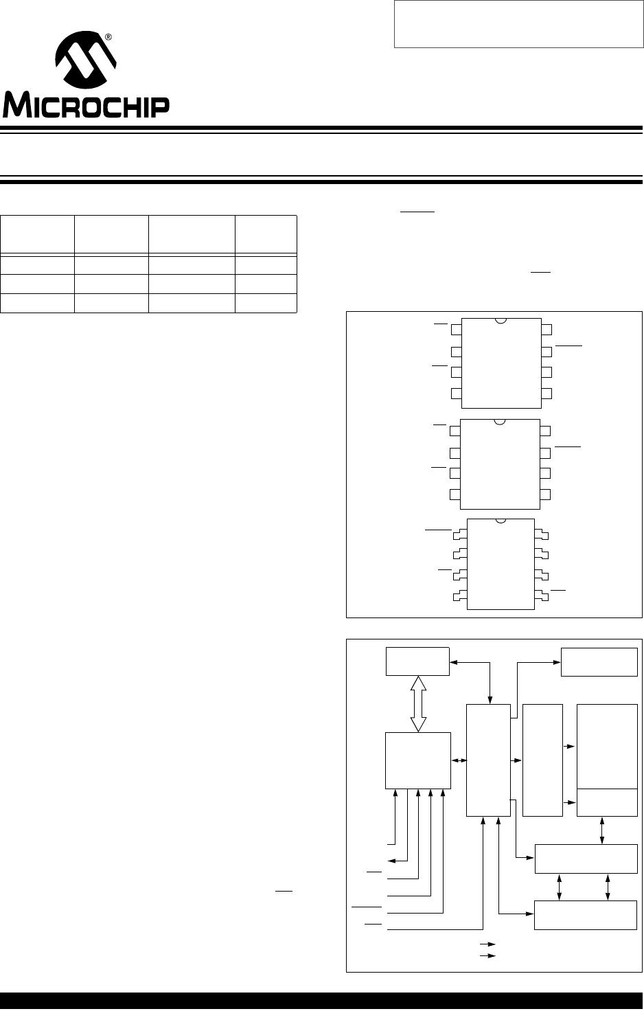
Device Selection Table
Features:
Low-power CMOS technology:
- Write current: 3 mA, typical
- Read current: 500 μA, typical
- Standby current: 500 nA, typical
512 x 8-bit organization
16 byte page
Write cycle time: 5 ms max.
Self-timed Erase and Write cycles
Block write protection:
- Protect none, 1/4, 1/2 or all of array
Built-in write protection:
- Power on/off data protection circuitry
- Write enable latch
- Write-protect pin
Sequential read
High reliability:
- Endurance: 1M cycles
- Data retention: > 200 years
- ESD protection: > 4000V
8-pin PDIP, SOIC and TSSOP packages
Temperature ranges supported:
Description:
The Microchip Technology Inc. 25AA040/25LC040/
25C040 (25XX040
*
) is a 4 Kbit serial Electrically
Erasable PROM. The memory is accessed via a simple
Serial Peripheral Interface (SPI) compatible serial bus.
The bus signals required are a clock input (SCK) plus
separate data in (SI) and data out (SO) lines. Access to
the device is controlled through a Chip Select (CS
)
input.
Communication to the device can be paused via the
hold pin (HOLD
). While the device is paused, transi-
tions on its inputs will be ignored, with the exception of
Chip Select, allowing the host to service higher priority
interrupts. Also, write operations to the device can be
disabled via the write-protect pin (WP).
Package Types
Block Diagram
Part
Number
VCC
Range
Max. Clock
Frequency
Temp.
Ranges
25AA040 1.8-5.5V 1 MHz I
25LC040 2.5-5.5V 2 MHz I
25C040 4.5-5.5V 3 MHz I,E
- Industrial (I): -40°Cto +85°C
- Automotive (E) (25C040): -40°C to +125°C
CS
SO
WP
VSS
VCC
HOLD
SCK
SI
1
2
3
4
8
7
6
5
25XX040
CS
SO
WP
VSS
VCC
HOLD
SCK
SI
1
2
3
4
8
7
6
5
25XX040
HOLD
VCC
CS
SO
1
2
3
4
8
7
6
5
SCK
SI
V
SS
WP
25XX040
PDIP
SOIC
TSSOP
SI
SO
SCK
CS
HOLD
WP
STATUS
Register
I/O Control
Memory
Control
Logic
HV Generator
EEPROM
Array
Page
Y Decoder
Sense Amp.
R/W Control
Logic
VCC
VSS
XDEC
Latches
4K SPI Bus Serial EEPROM
*25XX040 is used in this document as a generic part number
for the 25AA040/25LC040/25C040 devices.
Not recommended for new designs –
Please use 25AA040A or 25LC040A.
25AA040/25LC040/25C040
DS21204E-page 2 © 2006 Microchip Technology Inc.
1.0 ELECTRICAL CHARACTERISTICS
Absolute Maximum Ratings
(†)
VCC.............................................................................................................................................................................7.0V
All inputs and outputs w.r.t. V
SS .......................................................................................................... -0.6V to VCC+1.0V
Storage temperature .................................................................................................................................-65°C to 150°C
Ambient temperature under bias...............................................................................................................-65°C to 125°C
ESD protection on all pins......................................................................................................................................... 4 KV
TABLE 1-1: DC CHARACTERISTICS
† NOTICE: Stresses above those listed under “Absolute Maximum Ratings” may cause permanent damage to the
device. This is a stress rating only and functional operation of the device at those or any other conditions above those
indicated in the operational listings of this specification is not implied. Exposure to maximum rating conditions for an
extended period of time may affect device reliability
DC CHARACTERISTICS
Industrial (I): T
A = -40°C to +85°C VCC = 1.8V to 5.5V
Automotive (E): T
A = -40°C to +125°C VCC = 4.5V to 5.5V (25C040 only)
Param.
No.
Sym. Characteristic Min. Max. Units Test Conditions
D001 V
IH1 High-level input
voltage
2.0 VCC+1 V VCC2.7V (Note)
D002 VIH2 0.7 VCC VCC+1 V VCC< 2.7V (Note)
D003 V
IL1 Low-level input
voltage
-0.3 0.8 V VCC2.7V (Note)
D004 VIL2 -0.3 0.3 VCC VVCC < 2.7V (Note)
D005 VOL Low-level output
voltage
—0.4VIOL = 2.1 mA
D006 V
OL —0.2VIOL = 1.0 mA, VCC < 2.5V
D007 VOH High-level output
voltage
VCC -0.5 V IOH =-400 μA
D008 I
LI Input leakage current ±1 μACS = VCC, VIN = VSS TO VCC
D009 ILO Output leakage
current
—±1μACS = VCC, VOUT = VSS TO VCC
D010 CINT Internal Capacitance
(all inputs and
outputs)
—7pFT
A = 25°C, CLK = 1.0 MHz,
V
CC = 5.0V (Note)
D011 I
CC Read Operating Current
1
500
mA
μA
VCC = 5.5V; FCLK = 3.0 MHz; SO = Open
V
CC = 2.5V; FCLK = 2.0 MHz; SO = Open
D012 ICC Write
5
3
mA
mA
VCC = 5.5V
V
CC = 2.5V
D013 ICCS Standby Current
5
1
μA
μA
CS = VCC = 5.5V, Inputs tied to VCC or
V
SS
CS = VCC = 2.5V, Inputs tied to VCC or
V
SS
Note: This parameter is periodically sampled and not 100% tested.
© 2006 Microchip Technology Inc. DS21204E-page 3
25AA040/25LC040/25C040
TABLE 1-2: AC CHARACTERISTICS
AC CHARACTERISTICS
Industrial (I): T
A = -40°C to +85°C VCC = 1.8V to 5.5V
Automotive (E): T
A = -40°C to +125°C VCC = 4.5V to 5.5V (25C040 only)
Param
No.
Sym. Characteristic Min. Max. Units Test Conditions
1FCLK Clock Frequency
3
2
1
MHz
MHz
MHz
VCC = 4.5V to 5.5V
V
CC = 2.5V to 4.5V
V
CC = 1.8V to 2.5V
2T
CSS CS Setup Time 100
250
500
ns
ns
ns
VCC = 4.5V to 5.5V
V
CC = 2.5V to 4.5V
V
CC = 1.8V to 2.5V
3T
CSH CS Hold Time 150
250
475
ns
ns
ns
VCC = 4.5V to 5.5V
V
CC = 2.5V to 4.5V
V
CC = 1.8V to 2.5V
4T
CSD CS Disable Time 500 ns
5T
SU Data Setup Time 30
50
50
ns
ns
ns
VCC = 4.5V to 5.5V
V
CC = 2.5V to 4.5V
V
CC = 1.8V to 2.5V
6T
HD Data Hold Time 50
100
100
ns
ns
ns
VCC = 4.5V to 5.5V
V
CC = 2.5V to 4.5V
V
CC = 1.8V to 2.5V
7T
R CLK Rise Time 2 μs (Note 1)
8T
F CLK Fall Time 2 μs (Note 1)
9T
HI Clock High Time 150
230
475
ns
ns
ns
V
CC = 4.5V to 5.5V
V
CC = 2.5V to 4.5V
V
CC = 1.8V to 2.5V
10 T
LO Clock Low Time 150
230
475
ns
ns
ns
VCC = 4.5V to 5.5V
V
CC = 2.5V to 4.5V
V
CC = 1.8V to 2.5V
11 T
CLD Clock Delay Time 50 ns
12 T
CLE Clock Enable Time 50 ns
13 T
V Output Valid from Clock Low
150
230
475
ns
ns
ns
VCC = 4.5V to 5.5V
V
CC = 2.5V to 4.5V
V
CC = 1.8V to 2.5V
14 T
HO Output Hold Time 0 ns (Note 1)
15 T
DIS Output Disable Time
200
250
500
ns
ns
ns
V
CC = 4.5V to 5.5V (Note 1)
V
CC = 2.5V to 4.5V (Note 1)
V
CC = 1.8V to 2.5V (Note 1)
16 T
HS HOLD Setup Time 100
100
200
ns
ns
ns
VCC = 4.5V to 5.5V
V
CC = 2.5V to 4.5V
V
CC = 1.8V to 2.5V
17 T
HH HOLD Hold Time 100
100
200
ns
ns
ns
VCC = 4.5V to 5.5V
V
CC = 2.5V to 4.5V
V
CC = 1.8V to 2.5V
18 T
HZ HOLD Low to Output High-Z 100
150
200
ns
ns
ns
VCC = 4.5V to 5.5V (Note 1)
V
CC = 2.5V to 4.5V (Note 1)
V
CC = 1.8V to 2.5V (Note 1)
19 T
HV HOLD High to Output Valid 100
150
200
ns
ns
ns
VCC = 4.5V to 5.5V
V
CC = 2.5V to 4.5V
V
CC = 1.8V to 2.5V
20 T
WC Internal Write Cycle Time 5 ms
21 Endurance 1M E/W
Cycles
(Note 2)
Note 1: This parameter is periodically sampled and not 100% tested.
2: This parameter is not tested but ensured by characterization. For endurance estimates in a specific application, please
consult the Total Endurance™ Model which can be obtained from our web site: www.microchip.com.

25AA040T-I/SN

Mfr. #:
Manufacturer:
Microchip Technology
Description:
EEPROM 512x8 - 1.8V
Lifecycle:
New from this manufacturer.
Delivery:
DHL FedEx Ups TNT EMS
Payment:
T/T Paypal Visa MoneyGram Western Union