VS-ST330S14P0

VS-ST330SPbF Series
www.vishay.com
Vishay Semiconductors
Revision: 01-Mar-17
4
Document Number: 94409
For technical questions within your region: DiodesAmericas@vishay.com
, DiodesAsia@vishay.com, DiodesEurope@vishay.com
THIS DOCUMENT IS SUBJECT TO CHANGE WITHOUT NOTICE. THE PRODUCTS DESCRIBED HEREIN AND THIS DOCUMENT
ARE SUBJECT TO SPECIFIC DISCLAIMERS, SET FORTH AT www.vishay.com/doc?91000
Fig. 1 - Current Ratings Characteristics Fig. 2 - Current Ratings Characteristics
Fig. 3 - On-State Power Loss Characteristics
Fig. 4 - On-State Power Loss Characteristics
70
80
90
100
110
120
130
0 50 100 150 200 250 300 350
Maximum Allowable Case Temperature C)
30°
60°
90°
120°
180°
Average On-state Current (A)
Conduction Angle
ST3 3 0 S Se r i e s
R (DC) = 0.10 K/ W
thJC
60
70
80
90
100
110
120
130
0 100 200 300 400 500 600
DC
30°
60°
90°
120°
180°
Average On-state Current (A)
Maximum Allowable Case Temperature (°C)
Conduction Period
ST3 3 0 S Se r i e s
R (DC) = 0.10 K/W
thJC
25 50 75 100 125
Maximum Allowable Ambient Temperature (°C)
0
.
0
8
K
/
W
0
.
2
K
/
W
0
.
3
K
/
W
0
.
4
K
/
W
0
.
6
K
/
W
1
.
2
K
/
W
R
=
0
.
0
3
K
/
W
-
D
e
l
t
a
R
t
h
S
A
0
.
1
2
K
/
W
0
40
80
120
160
200
240
280
320
360
400
440
480
0 50 100 150 200 250 300 350
180°
120°
90°
60°
30°
RM S Li m it
Conduction Angle
Maximum Average On-state Power Loss (W)
Average On-state Current (A)
ST3 3 0 S Se r i e s
T = 1 2 5 ° C
J
25 50 75 100 125
Maximum Allowable Ambient Temperature (°C)
R
=
0.0
3 K/ W
-
De
lta R
t
hS
A
0
.
0
8
K
/
W
0
.
1
2
K
/
W
0
.
2
K
/
W
0
.
3
K
/
W
0
.
4
K
/
W
0
.
6
K
/
W
1
.
2
K
/
W
0
50
100
150
200
250
300
350
400
450
500
550
600
650
0 100 200 300 400 500 600
DC
180°
120°
90°
60°
30°
RM S Li m i t
Conduction Period
Maximum Average On-state Power Loss (W)
Average On-state Current (A)
ST3 3 0 S Se r i e s
T = 125°C
J
VS-ST330SPbF Series
www.vishay.com
Vishay Semiconductors
Revision: 01-Mar-17
5
Document Number: 94409
For technical questions within your region: DiodesAmericas@vishay.com
, DiodesAsia@vishay.com, DiodesEurope@vishay.com
THIS DOCUMENT IS SUBJECT TO CHANGE WITHOUT NOTICE. THE PRODUCTS DESCRIBED HEREIN AND THIS DOCUMENT
ARE SUBJECT TO SPECIFIC DISCLAIMERS, SET FORTH AT www.vishay.com/doc?91000
Fig. 5 - Maximum Non-Repetitive Surge Current Fig. 6 - Maximum Non-Repetitive Surge Current
Fig. 7 - On-State Voltage Drop Characteristics
Fig. 8 - Thermal Impedance Z
thJC
Characteristics
3500
4000
4500
5000
5500
6000
6500
7000
7500
8000
110100
Number Of Equa l Amplitud e Half Cyc le Current Pulses (N)
Peak Half Sine Wave On-sta te Current (A)
Initial T = 125°C
@ 60 Hz 0.0083 s
@ 50 Hz 0.0100 s
J
ST3 3 0 S Se r i e s
At Any Rated Load Condition And With
Rated V Applied Following Surge.
RRM
3000
4000
5000
6000
7000
8000
9000
0.01 0.1 1
Pulse Train Duration (s)
Versus Pulse Train Duration. Control
Pe a k Ha lf Sine Wa v e O n -st a t e C urr e nt ( A)
Initia l T = 125°C
No Voltage Reapplied
Rated V Reapplied
RRM
J
ST330S Series
Maximum Non Repetitive Surge Current
Of Conduction May Not Be Maintained.
Instantaneous On-state Voltage (V)
Instantaneous On-state Current (A)
100
1000
10000
0 1 2 3 4 5 6 7
Tj = 25 °C
Tj = 125 °C
ST330S Series
0.001
0.01
0.1
1
0.001 0.01 0.1 1 10
Sq u a r e W a v e P u l se D u r a t i o n ( s)
thJC
ST3 3 0 S Se r i e s
St e a d y St a t e V a l u e
R = 0.10 K/ W
(DC Operation)
thJC
Transient Thermal Impedance Z (K/W)
VS-ST330SPbF Series
www.vishay.com
Vishay Semiconductors
Revision: 01-Mar-17
6
Document Number: 94409
For technical questions within your region: DiodesAmericas@vishay.com
, DiodesAsia@vishay.com, DiodesEurope@vishay.com
THIS DOCUMENT IS SUBJECT TO CHANGE WITHOUT NOTICE. THE PRODUCTS DESCRIBED HEREIN AND THIS DOCUMENT
ARE SUBJECT TO SPECIFIC DISCLAIMERS, SET FORTH AT www.vishay.com/doc?91000
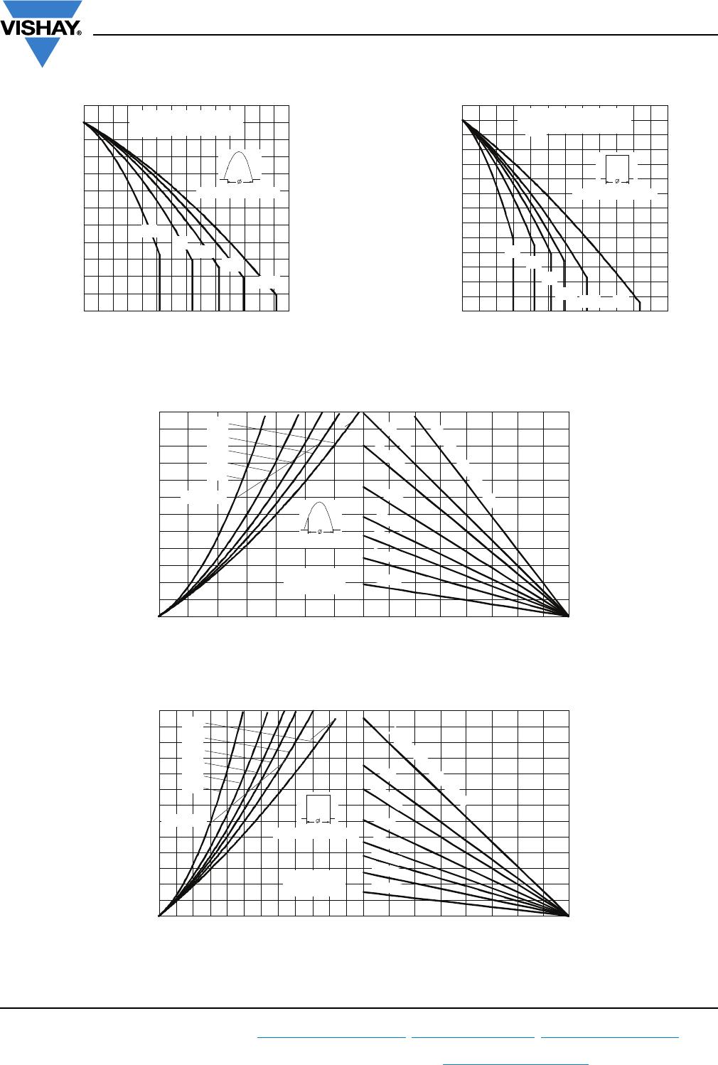
Fig. 9 - Gate Characteristics
ORDERING INFORMATION TABLE
0.1
1
10
100
0.001 0.01 0.1 1 10 100
VGD
IGD
(b)
(a)
Tj = 2 5 ° C
Tj = 1 2 5 ° C
Tj = - 4 0 ° C
(2)
(3)
In st a n t a n e o u s G a t e C u rre n t ( A )
Inst a nt an eo us G a t e Vo lt a g e (V)
Rectangular gate pulse
a) Recommended load line for
b) Recommended load line for
<=30% rated di/dt : 10V, 10ohms
Frequency Limited by PG(AV)
rated d i/ dt : 20V, 10ohms; tr<=1 µs
tr<=1 µs
(1)
(1) PGM = 10W, tp = 4ms
(2) PGM = 20W, tp = 2ms
(3) PGM = 40W, tp = 1ms
(4) PGM = 60W, t p = 0.66m s
D e v i c e : ST3 3 0 S Se r i e s
(4)
- Thyristor
2
- Essential part number
3
- 0 = converter grade
4
- S = compression bonding stud
5
- Voltage code x 100 = V
RRM
(see Voltage Ratings table)
6
- P = stud base 3/4"-16UNF-2A threads
7
- 0 = eyelet terminals (gate and auxiliary cathode leads)
1 = fast-on terminals (gate and auxiliary cathode leads)
9
8
Device code
51 32 4 6 7 8 9
STVS- 33 0 S 16 P 0 PbF
1 - Vishay Semiconductors product
- None = standard production
- PbF = lead (Pb)-free
M = stud base metric threads (M24 x 1.5)
LINKS TO RELATED DOCUMENTS
Dimensions www.vishay.com/doc?95080

VS-ST330S14P0

Mfr. #:
Manufacturer:
Vishay Semiconductors
Description:
SCR Modules Thyristors - TO-118 COMP RND-e3
Lifecycle:
New from this manufacturer.
Delivery:
DHL FedEx Ups TNT EMS
Payment:
T/T Paypal Visa MoneyGram Western Union