X28HC64
13
FN8109.4
June 27, 2016
Submit Document Feedback
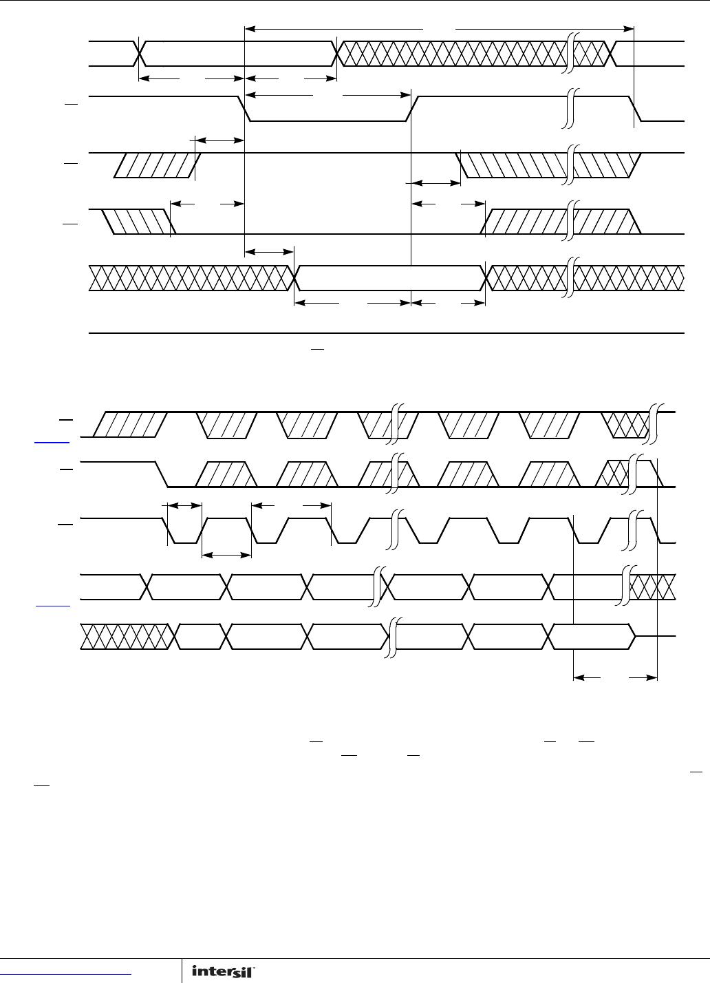
FIGURE 16. CE CONTROLLED WRITE CYCLE
FIGURE 17. PAGE WRITE CYCLE
NOTES:
17. Between successive byte writes within a page write operation, OE
can be strobed LOW: e.g. this can be done with CE and WE HIGH to fetch data from
another memory device within the system for the next write; or with WE
HIGH and CE LOW effectively performing a polling operation.
18. The timings shown above are unique to page write operations. Individual byte load operations within the page write must conform to either the CE
or WE
controlled write cycle timing.
ADDRESS
t
AS
t
OEH
t
WC
t
AH
t
OES
t
CS
t
DS
t
DH
t
CH
CE
WE
OE
DATA IN
DATA OUT
HIGH Z
DATA VALID
t
CW
t
DV
WE
OE
LAST BYTE
Byte 0 Byte 1 Byte 2 Byte n Byte n+1 Byte n+2
t
WP
t
WPH
t
BLC
t
WC
CE
ADDRESS
I/O
*For each successive write within the page write operation, A
6
–A
12
should be the same or
writes to an unknown address could occur.
Note 17
Note 18
X28HC64
14
FN8109.4
June 27, 2016
Submit Document Feedback
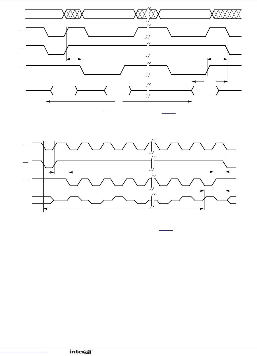
FIGURE 18. DATA POLLING TIMING DIAGRAM (Note 19)
FIGURE 19. TOGGLE BIT TIMING DIAGRAM (Note 19
)
NOTE:
19. Polling operations are by definition read cycles and are therefore subject to read cycle timings.
ADDRESS A
n
D
IN
= X
D
OUT
= X
t
OEH
t
OES
A
n
A
n
CE
WE
OE
I/O
7
t
DW
D
OUT
= X
t
WC
CE
OE
WE
I/O*
6
t
OES
t
DW
t
OEH
HIGH Z
*
*
* I/O
6
beginning and ending state will vary, depending upon actual t
WC
.
t
WC
X28HC64
15
FN8109.4
June 27, 2016
Submit Document Feedback
About Intersil
Intersil Corporation is a leading provider of innovative power management and precision analog solutions. The company's products
address some of the largest markets within the industrial and infrastructure, mobile computing and high-end consumer markets.
For the most updated datasheet, application notes, related documentation and related parts, please see the respective product
information page found at www.intersil.com.
You may report errors or suggestions for improving this datasheet by visiting www.intersil.com/ask
.
Reliability reports are also available from our website at www.intersil.com/support.
Revision History The revision history provided is for informational purposes only and is believed to be accurate, but not warranted.
Please go to the web to make sure that you have the latest revision.
DATE REVISION CHANGE
June 27, 2016 FN8109.4 Updated entire datasheet applying Intersil’s new standards.
Updated the Ordering Information table by adding Note 2, updated other tape and reel notes, updated all of the
part marking and added Note 6.
Added Thermal Information (Theta JA, Theta JC, and applicable notes) on page 9.
Added “The endurance and data retention specifications are established by characterization and are not
production tested” to the “Endurance and Data Retention” table.
August 18, 2015 FN8109.3 - Updated Ordering Information Table on page 2.
- Added Revision History and About Intersil sections.
- Updated POD M28.3 to latest revision changes are as follow:
Added land pattern.
X28HC64JIZ-90

Mfr. #:
Manufacturer:
Renesas / Intersil
Description:
EEPROM 8K X 8 EEPROM CMOS 3
Lifecycle:
New from this manufacturer.
Delivery:
DHL FedEx Ups TNT EMS
Payment:
T/T Paypal Visa MoneyGram Western Union

Products related to this Datasheet