X28HC64
9
FN8109.4
June 27, 2016
Submit Document Feedback
Absolute Maximum Ratings Thermal Information
Temperature Under Bias
X28HC64 . . . . . . . . . . . . . . . . . . . . . . . . . . . . . . . . . . . . . . . -10°C to +85°C
X28HC64I . . . . . . . . . . . . . . . . . . . . . . . . . . . . . . . . . . . . .-65°C to +135°C
Storage Temperature . . . . . . . . . . . . . . . . . . . . . . . . . . . . . .-65°C to +150°C
Voltage on any Pin with Respect to V
SS
. . . . . . . . . . . . . . . . . . . . .-1V to +7V
DC Output Current . . . . . . . . . . . . . . . . . . . . . . . . . . . . . . . . . . . . . . . . . . 5mA
Thermal Resistance (Typical)
JA
(°C/W)
JC
(°C/W)
32 Ld PLCC Package (Notes 7
, 9) . . . . . . . 41 19
28 Ld SOIC Package (Notes 7
, 9) . . . . . . . . 46 19
28 Ld PDIP Package (Notes 8
, 9). . . . . . . . 53 21
Pb-Free Reflow Profile . . . . . . . . . . . . . . . . . . . . . . . . . . . . . . . . . . see TB493
*Pb-free PDIPs can be used for through hole wave solder processing only.
They are not intended for use in Reflow solder processing applications.
Recommended Operating Conditions
Commercial Temperature Range . . . . . . . . . . . . . . . . . . . . . . 0°C to +70°C
Industrial Temperature Range . . . . . . . . . . . . . . . . . . . . . . . -40°C to +85°C
Supply Voltage Range
X28HC64 . . . . . . . . . . . . . . . . . . . . . . . . . . . . . . . . . . . . . . . . . . . . . 5V ±10%
CAUTION: Do not operate at or near the maximum ratings listed for extended periods of time. Exposure to such conditions may adversely impact product
reliability and result in failures not covered by warranty.
NOTES:
7.
JA
is measured with the component mounted on a high effective thermal conductivity test board in free air. See Tech Brief TB379 for details.
8.
JA
is measured with the component mounted on a low effective thermal conductivity test board in free air. See Tech Brief TB379 for details.
9. For
JC
, the “case temp” location is taken at the package top center.
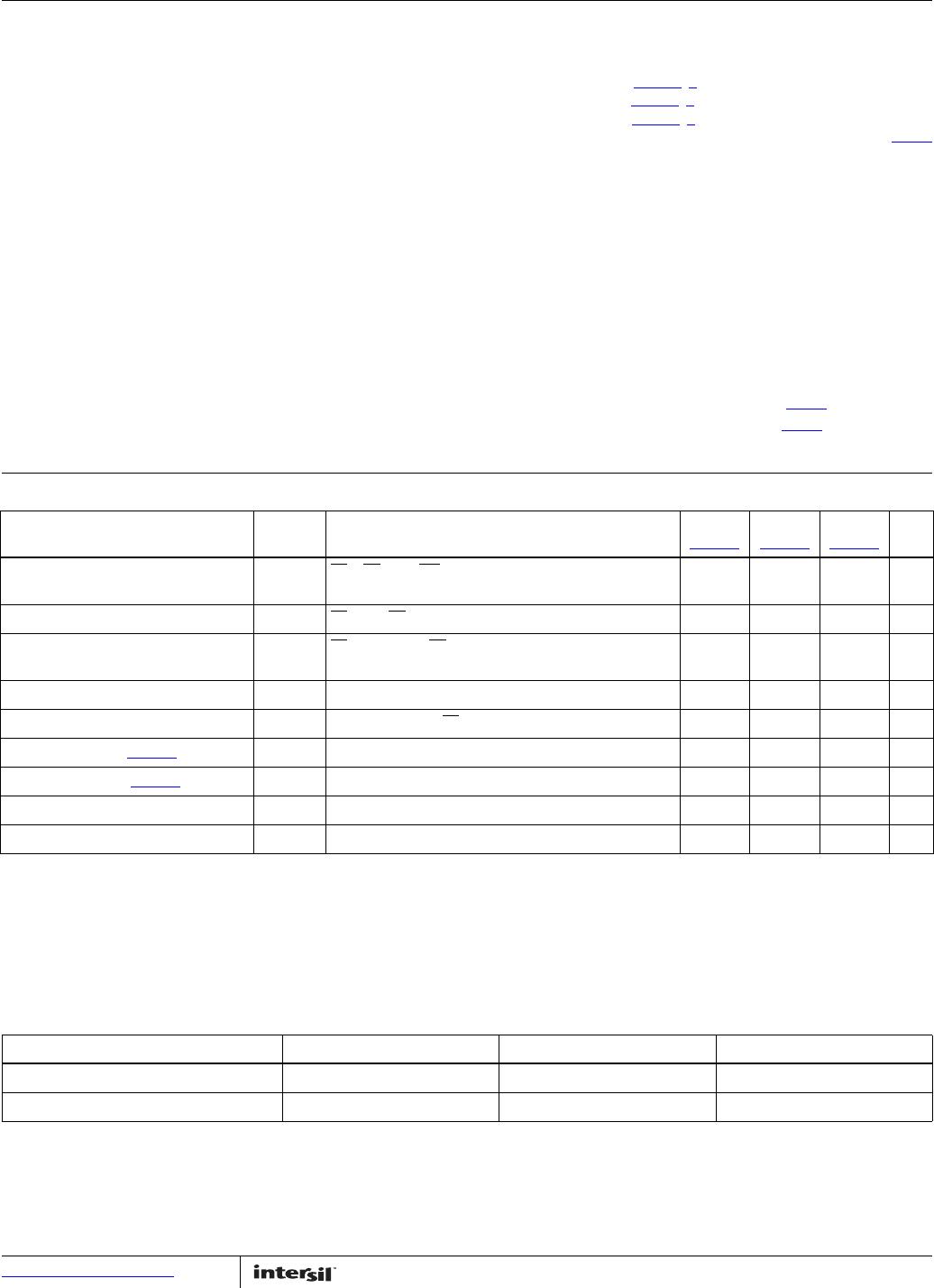
DC Electrical Specifications Over recommended operating conditions, unless otherwise specified.
PARAMETER SYMBOL TEST CONDITIONS
MIN
(Note 10
)
TYP
(Note 11)
MAX
(Note 10)UNIT
V
CC
Current (Active) (TTL Inputs) I
CC
CE = OE = V
IL
, WE = V
IH
, All I/O’s = open, address
inputs = TTL levels at f = 10MHz
15 40 mA
V
CC
Current (Standby) (TTL Inputs) I
SB1
CE = V
IH
, OE = V
IL
All I/O’s = open, other inputs = V
IH
12mA
V
CC
Current (Standby) (CMOS Inputs) I
SB2
CE = V
CC
- 0.3V, OE = GND, All I/O’s = open, other
inputs = V
CC
- 0.3V
100 200 µA
Input Leakage Current I
LI
V
IN
= V
SS
to V
CC
±10 µA
Output Leakage Current I
LO
V
OUT
= V
SS
to V
CC
, CE = V
IH
±10 µA
Input LOW Voltage (Note 12
)V
lL
-1 0.8 V
Input HIGH Voltage (Note 12
)V
IH
2V
CC
+ 1 V
Output LOW Voltage V
OL
I
OL
= 5mA 0.4 V
Output HIGH Voltage V
OH
I
OH
= -5mA 2.4 V
NOTES:
10. Parameters with MIN and/or MAX limits are 100% tested at +25°C, unless otherwise specified. Temperature limits established by characterization
and are not production tested.
11. Typical values are for T
A
= +25°C and nominal supply voltage.
12. V
IL
minimum and V
IH
maximum are for reference only and are not tested.
Endurance and Data Retention The endurance and data retention specifications are established by characterization and are not
production tested.
PARAMETER MIN MAX UNIT
Minimum Endurance 100,000 Cycles
Data Retention 100 Years