VBT6045C-E3
www.vishay.com
Vishay General Semiconductor
Revision: 09-Sep-13
1
Document Number: 89362
For technical questions within your region: DiodesAmericas@vishay.com
, DiodesAsia@vishay.com, DiodesEurope@vishay.com
THIS DOCUMENT IS SUBJECT TO CHANGE WITHOUT NOTICE. THE PRODUCTS DESCRIBED HEREIN AND THIS DOCUMENT
ARE SUBJECT TO SPECIFIC DISCLAIMERS, SET FORTH AT www.vishay.com/doc?91000
Dual Low-Voltage Trench MOS Barrier Schottky Rectifier
Ultra Low V
F
= 0.33 V at I
F
= 10 A
FEATURES
• Trench MOS Schottky technology
• Low forward voltage drop, low power losses
• High efficiency operation
• Meets MSL level 1, per J-STD-020, LF maximum
peak of 245 °C
• Material categorization: For definitions of compliance
please see www.vishay.com/doc?99912
TYPICAL APPLICATIONS
For use in high frequency DC/DC converters, switching
power supplies, freewheeling diodes, OR-ing diode, and
reverse battery protection.
MECHANICAL DATA
Case: TO-263AB
Molding compound meets UL 94 V-0 flammability rating
Base P/N-E3 - RoHS-compliant, commercial grade
Terminals: Matte tin plated leads, solderable per
J-STD-002 and JESD 22-B102
E3 suffix meets JESD 201 class 1A whisker test
Polarity: As marked
Mounting Torque: 10 in-lbs maximum
PRIMARY CHARACTERISTICS
I
F(AV)
2 x 30 A
V
RRM
45 V
I
FSM
320 A
V
F
at I
F
= 30 A 0.47 V
T
J
max. 150 °C
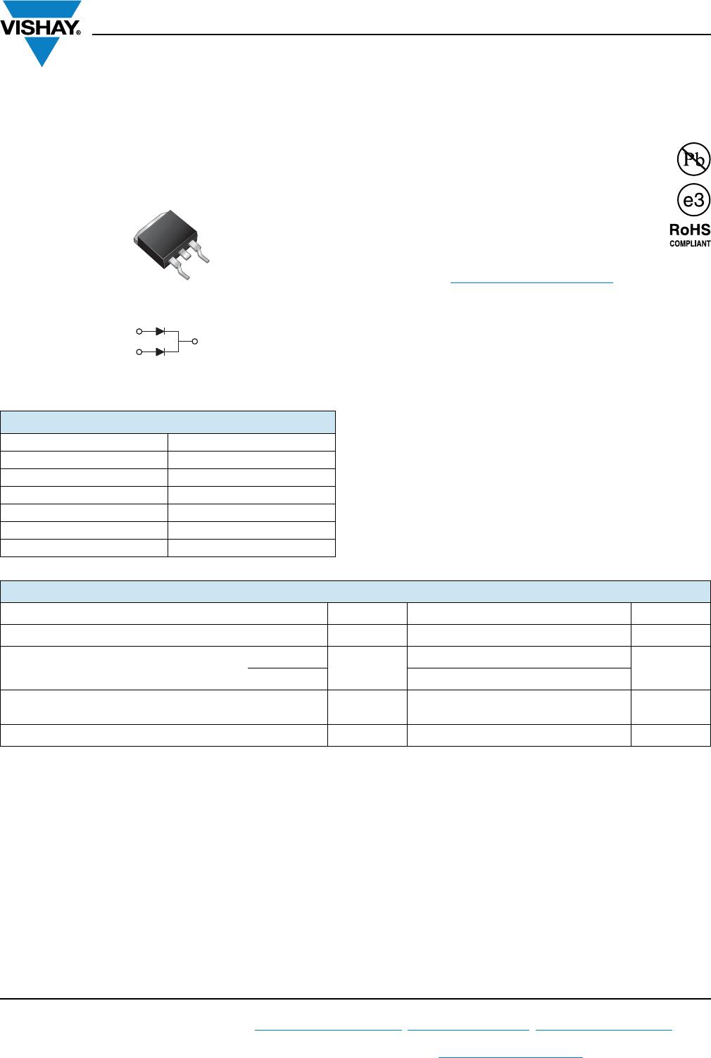
Package TO-263AB
Diode variations Common cathode
TO-263AB
1
2
K
PIN 1
PIN 2
K
HEATSINK
VBT6045C
TMBS
®
MAXIMUM RATINGS (T
A
= 25 °C unless otherwise noted)
PARAMETER SYMBOL VBT6045C UNIT
Maximum repetitive peak reverse voltage V
RRM
45 V
Maximum average forward rectified current
(fig. 1)
per device
I
F(AV)
60
A
per diode 30
Peak forward surge current 8.3 ms single half sine-wave
superimposed on rated load
I
FSM
320 A
Operating junction and storage temperature range T
J
, T
STG
-40 to +150 °C