LTC4219
13
4219fd
For more information www.linear.com/LTC4219
applicaTions inFormaTion
1.235V for a minimum of 5µs and then low will clear the
fault latch. If the TIMER pin is tied to INTV
CC
then the
switch is allowed to turn on again (after an internal 100ms
delay), if the overcurrent fault latch is cleared.
Tying the P-channel MOSFET Q1 to the EN1 pin allows
the part to self-clear the fault and turn the MOSFET on as
soon as the TIMER pin has ramped below 0.21V. In the
auto-retry mode the LTC4219 repeatedly tries to turn on
after an overcurrent at a period determined by the capaci
-
tor on the TIMER pin. The auto-retry mode also functions
when the TIMER pin is tied to INT
V
CC
.
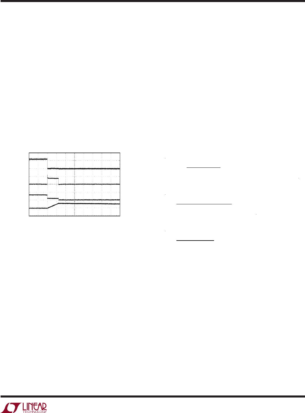
The waveform in Figure 4 shows how the output latches
off following a short-circuit. The current in the MOSFET
is 1.4A as the timer ramps up.
The overall current limit threshold precision is reduced to
±12% when using a 20k resistor to halve the threshold.
Using a switch (connected to ground) in series with R
SET
allows the active current limit to change only when the
switch is closed. This feature can be used to program a
reduced running current while the maximum available
current limit is used at startup.
Monitor MOSFET Temperature
The voltage at the I
SET
pin increases linearly with increas-
ing temperature. The temperature profile of the I
SET
pin is
shown in the Typical Performance Characteristics section.
Using a comparator or ADC to measure the I
SET
voltage
provides an indicator of the MOSFET temperature.
The I
SET
voltage follows the formula:
V
ISET
=
R
SET
R
SET
+R
ISET
(T+ 273°C) 2.093[mV/°C]
The MOSFET temperature is calculated using R
ISET
of 20k.
T =
(R
SET
+
20k) V
ISET
R
SET
2.093[mV/°C]
273°C
when R
SET
is not present, T becomes:
T =
V
ISET
2.093[mV/°C]
273°C
There is an overtemperature circuit in the LTC4219 that
monitors an internal voltage similar to the I
SET
pin voltage.
When the die temperature exceeds 145°C the circuit turns
off the MOSFET until the temperature drops to 125°C.
Monitor MOSFET Current
The current in the MOSFET passes through an internal
7.5mΩ sense resistor. The voltage on the sense resistor is
converted to a current that is sourced out of the I
MON
pin.
The gain of I
SENSE
amplifier is 20µA/A referenced from the
MOSFET current. This output current can be converted to
a voltage using an external resistor to drive a comparator
or ADC. The voltage compliance for the I
MON
pin is from
0V to INTV
CC
– 0.7V.
Figure 4. Short-Circuit Waveform
AV
GATE
10V/DIV
I
OUT
2A/DIV
V
OUT
10V/DIV
TIMER
2V/DIV
1ms/DIV
4219 F04
Current Limit Adjustment
The default value of the active current limit is 5.6A. The
current limit threshold can be adjusted lower by placing
a resistor between the I
SET
pin and ground. As shown in
the Functional Block Diagram the voltage at the I
SET
pin
(via the clamp circuit) sets the CS amplifiers built-in offset
voltage. This offset voltage directly determines the active
current limit value. With the I
SET
pin open, the voltage at
the I
SET
pin is determined by a positive temperature co-
efficient reference. This voltage is set to 0.618V at room
temperature which corresponds to a 5.6
A current limit at
room temperature.
An external resistor R
SET
placed between the I
SET
pin and
ground forms a resistive divider with the internal 20k R
ISET
sourcing resistor. The divider acts to lower the voltage at
the I
SET
pin and therefore lower the current limit threshold.
LTC4219
14
4219fd
For more information www.linear.com/LTC4219
applicaTions inFormaTion
A microcontroller with a built-in comparator can build a
simple integrating single-slope ADC by resetting a capaci-
tor that is charged with this current. When the capacitor
voltage trips the comparator and the capacitor is reset
,
a
timer is started. The time between resets will indicate the
MOSFET current.
Power Good Indication
In addition to setting the foldback current limit threshold,
the FB pin is used to determine a power good condition.
The LTC4219-12 and LTC4219-5 use an internal resis
-
tive divider on the OUT pin to drive the FB pin. On the
LTC4219-12,
the PG comparator indicates logic high when
OUT pin rises above 10.5V. If the OUT pin subsequently
falls below 10.3V, the comparator toggles low. On the
LTC4219-5 the PG comparator drives high when the OUT
pin rises above 4.35V and low when OUT falls below 4.27V.
Once the PG comparator is high, the GATE pin voltage is
monitored with respect to the OUT pin. Once the GATE
minus OUT voltage exceeds 4.2V, the PG pin goes low.
This indicates to the system that it is safe to load the OUT
pin while the MOSFET is completely turned “on”. The PG
pin goes high when the GATE is commanded off (using
the EN1, EN2 or SENSE pins) or when the PG comparator
drives low.
Design Example
Consider the following design example (Figure 5): V
IN
= 12V,
I
MAX
= 5A. I
INRUSH
= 100mA, C
L
= 330µF, V
PGTHRESHOLD
= 10.5V.
The inrush current is defined by the current required to
charge the output capacitor using the fixed 0.3V/
ms GATE
charge up rate. The inrush current is defined as:
I
INRUSH
=
C
L
0.3[V/ms]
=
330µF 0.3[V/ms]
=
100mA
As mentioned previously, the charge up time is the out-
put voltage (12V) divided by the output rate of 0.3V/ms
resulting in 40ms.
The peak power dissipation of 12V at
100mA (or 1.2W) is within the SOA of the pass MOSFET
for 40ms (see MOSFET SOA curve in the Typical Perfor
-
mance Characteristics section).
Next the
power dissipated in the MOSFET during overcur-
rent must be limited. The active current limit uses a timer
to prevent excessive energy dissipation in the MOSFET.
The worst-case power dissipation occurs when the voltage
versus current profile of the foldback current limit is at the
maximum. This occurs when the current is 6.1A and the
voltage is one half of the V
IN
or 6V. See the Current Limit
Threshold Foldback vs FB Voltage in the Typical Perfor-
mance Characteristics section to view this profile. In order
to sur
vive
36W, the MOSFET SOA dictates a maximum
time of 10ms (see SOA graph). Use the internal 2ms timer
invoked by tying the TIMER pin to INTV
CC
.
Figure 5. 5A, 12V Card Resident Application
ADC
C1
F
12V
V
OUT
12V
5A
R
MON
20k
4219 F05
R4
10k
PG = 10.5V
12V
R1
10k
C
L
330µF
V
DD
OUT
GATE
PG
GND
I
MON
I
SET
LTC4219DHC-12
INTV
CC
TIMER
EN1
EN2
F LT
+
Z1*
R3
200k
R2
200k
*TVS Z1: DIODES INC. SMAJ17A
LTC4219
15
4219fd
For more information www.linear.com/LTC4219
applicaTions inFormaTion
The power good threshold using the internal resistive
divider on the FB pin matches the 10.5V requirement.
The final schematic in Figure 5 results in very few external
components. The pull-up resistors, R1 and R4, connect
to the F LT and PG pins while the 20k (R
MON
) converts the
I
MON
current to a voltage at a ratio:
V
IMON
=
20 µA/A
[ ]
20k I
OUT
=
0.4 V/A
[ ]
I
OU
T
In addition there is a F bypass (C1) on the INTV
CC
pin.
Layout Considerations
In Hot Swap applications where load currents can be 5A,
narrow PCB tracks exhibit more resistance than wider tracks
and operate at elevated temperatures. The minimum trace
width for 1oz copper foil is 0.02" per amp to make sure
the trace stays at a reasonable temperature. Using 0.03"
per amp or wider is recommended. Note that 1oz copper
exhibits a sheet resistance of about 0.5mW/square. Small
resistances add up quickly in high current applications.
There are two V
DD
pins on opposite sides of the package
that connect to the sense resistor and MOSFET. The PCB
layout should be balanced and symmetrical to each V
DD
pin to balance current in the MOSFET bond wires. Figure 6
shows a recommended layout for the LTC4219.
Although the MOSFET is self protected from overtem
-
perature, it is recommended to solder the backside of the
package to a copper trace to provide a good heat sink.
Note that the backside is connected to the SENSE pin and
cannot be soldered to the ground plane
. During normal
loads the power dissipated in the package is as high as
1.9W. A 10mm × 10mm area of 1oz copper should be suf
-
ficient. This area of copper can be divided in many layers.
It is also important to put C1,
the bypass capacitor for
the INTV
CC
pin as close as possible between the INTV
CC
and GND.
Figure 6. Recommended Layout
4217 F06
HEAT SINK
VIA TO
SINK
GND
C
OUTV
DD
C1
F
5V
5V
R
MON
20k
4219 F07
R4
10k
PG = 4.35V
R1
10k
C
L
100µF
V
DD
EN1
EN2
OUT
GATE
PG
GND
I
MON
I
SET
LTC4219DHC-5
INTV
CC
TIMER
F LT
+
V
OUT
5V
5A
ADC
* TVS Z1: DIODES INC. SMAJ17A
Z1*
R3
200k
R2
200k
Additional Applications
The LTC4219 has a wide operating range from 2.9V to 15V.
The PG threshold is set with an internal resistive divider.
All other functions are independent of supply voltage.
Figure 7 shows a 5V application with a PG threshold of
4.35V.
In addition to Hot Swap applications, the LTC4219 also
functions as a backplane resident switch for removable
load cards (see the Typical Application section).
Figure 7. 5V, 5A Card Resident Application

LTC4219IDHC-5#TRPBF

Mfr. #:
Manufacturer:
Analog Devices Inc.
Description:
Hot Swap Voltage Controllers 5V, 5A Integrated Hot Swap Controller
Lifecycle:
New from this manufacturer.
Delivery:
DHL FedEx Ups TNT EMS
Payment:
T/T Paypal Visa MoneyGram Western Union