TISP4P015L1N THRU TISP4P035L1N
LOW CAPACITANCE
BIDIRECTIONAL THYRISTOR OVERVOLTAGE PROTECTOR
TISP4P0xxL1N Overvoltage Protector Series
OCTOBER 2009
*RoHS Directive 2002/95/EC Jan 27 2003 including Annex.
Specifi cations are subject to change without notice.
Customers should verify actual device performance in their specifi c applications.
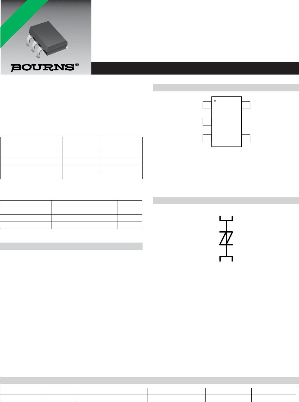
SOT23-5 Package (Top View)
This range of devices is designed to protect xDSL line-driver
interfaces from overvoltages up to rated limits. Overvoltages are
normally caused by a.c. power-system or lightning-fl ash distur-
bances which are induced or conducted onto the telephone line.
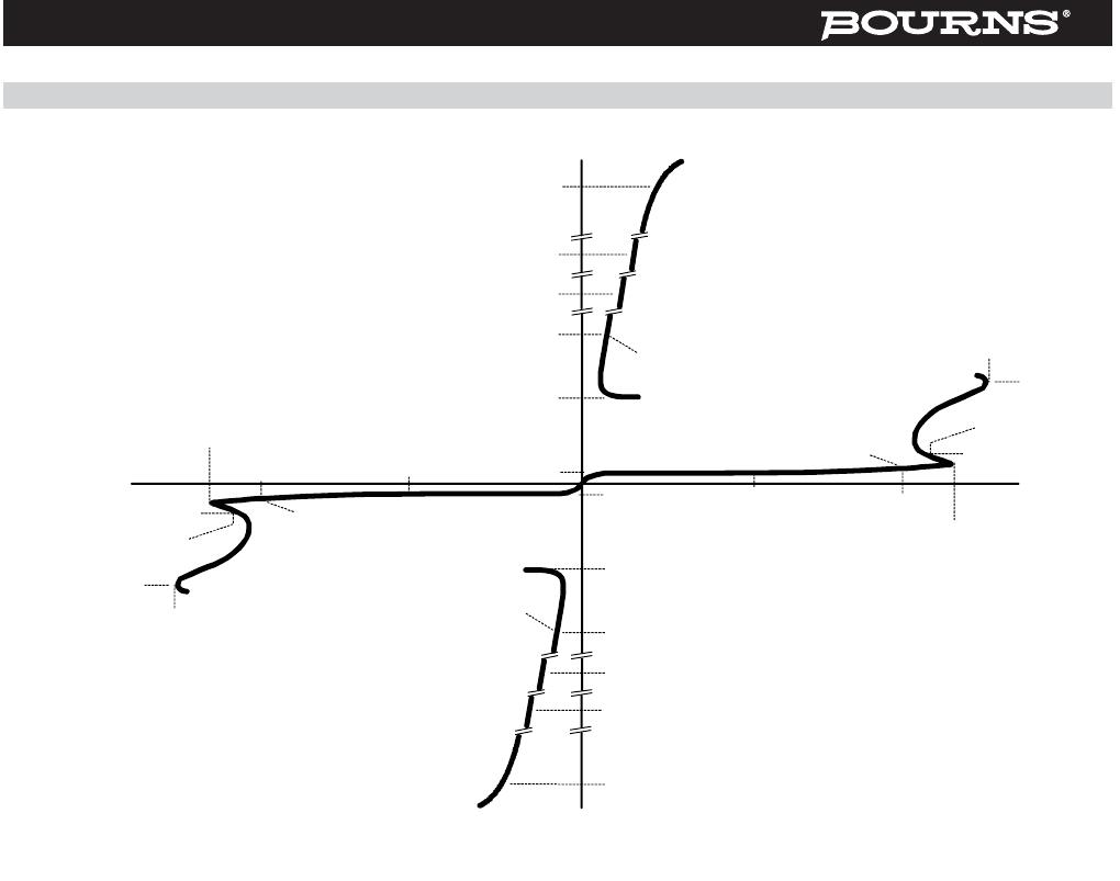
These symmetrical protectors are two-terminal thyristor-crowbar
devices. They can be used to protect between conductors, or a
pair of devices can be deployed to protect from line to ground.
Designed for ADSL, ADSL2, VDSL, VDSL2 protection
Ion-Implanted Breakdown Region
- Precise and Stable Voltage
Low Voltage Overshoot Under Surge
Low Off-State Capacitance
Rated for International Surge Wave Shapes
Device Symbol
Description
When placed between the xDSL line driver IC and the transformer, this protector will clamp and switch into a low-impedance state,
safely diverting the energy transferred by the xDSL coupling transformer. The low capacitance design makes this device suitable for
designs from ADSL all the way up to 30 MHz VDSL2.
Telecom ports need protection against Common Mode (Longitudinal) and Differential (Metallic) surges, to comply with international
standards such as ITU-T K.20, K.21 or K.45, Telcordia GR-1089-CORE and YD/T. Common Mode surges are resisted by the galvanic
isolation of the coupling transformer which is commonly rated to 2 kV or greater. Differential surges can be transmitted by the
transformer, and can stress the Line Driver Interface IC. As the xDSL interface circuit is designed to operate from 3 kHz to to 30 MHz,
nearby high frequency events - such as cable fl ashover or primary protection activation - can generate damaging conditions for the
interface requiring this type of protection.
Please contact your Bourns representative if the protection voltage you require is not listed.
How to Order
Device Name
V
DRM
V
V
(BO)
V
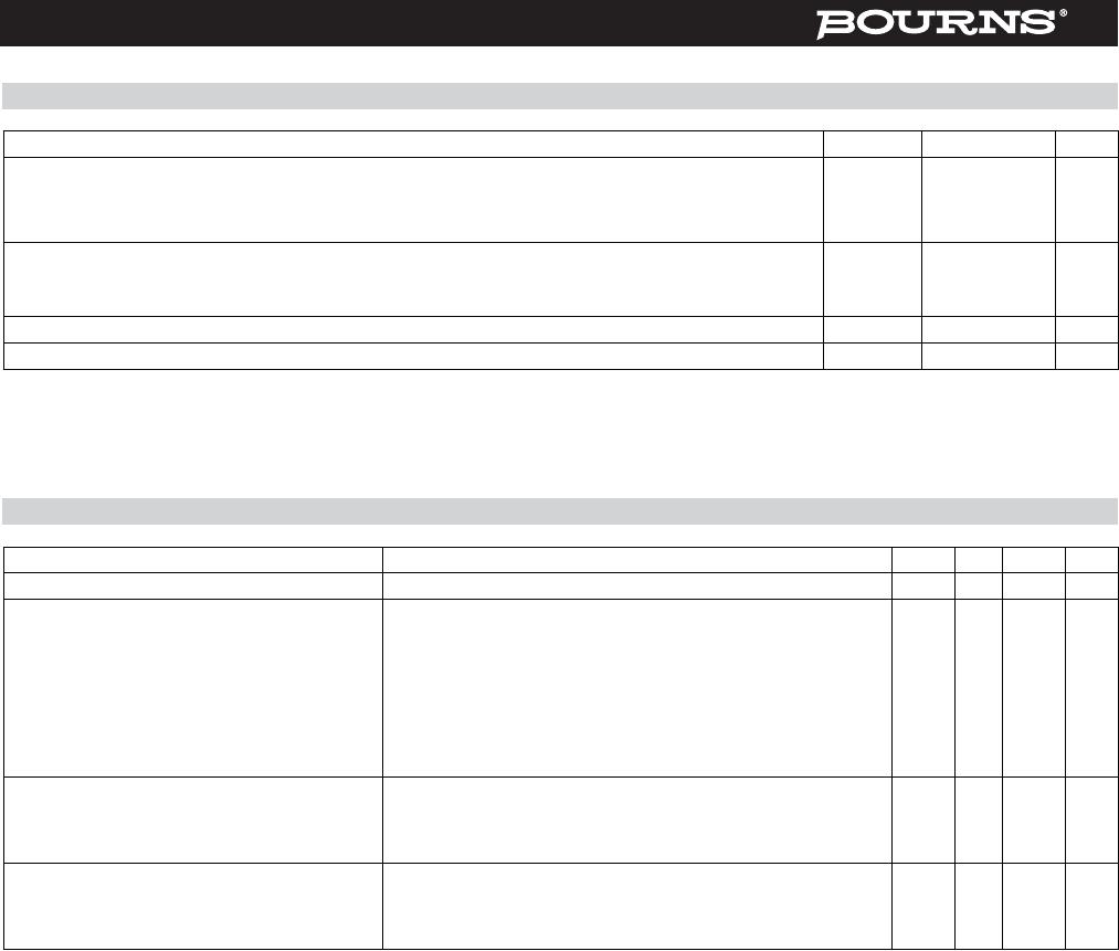
TISP4P015L1N 8 15
TISP4P020L1N 12 20
TISP4P025L1N 16 25
TISP4P035L1N 24
35
Wave Shape Standard
I
PPSM
A
8/20 IEC 61000-4-5 30
10/1000 GR-1089-CORE 18
MD-SOT23-5-001-a
Terminal typical application names
shown in parenthesis.
NU - Non-usable; no external electrical
connection should be made to this terminal.
(Ring)
1
2
34
5)piT()piT(
(Ring)
NU
(Tip)
SD-TISP4-002-a
(Ring)
ytitnauQ leeRedoC gnikraMsA redrOreirraCegakcaPeciveD
TISP4P0xxL1N SOT23-5 Embossed Tape Reeled TISP4P0xxL1NR-S Pxx 10000
Insert xx corresponding to device name.