Electrical Specifications
Stresses greater than those listed may cause permanent damage to the module. This is a
stress rating only, and functional operation of the module at these or any other condi-
tions outside those indicated in each device's data sheet is not implied. Exposure to ab-
solute maximum rating conditions for extended periods may adversely affect reliability.
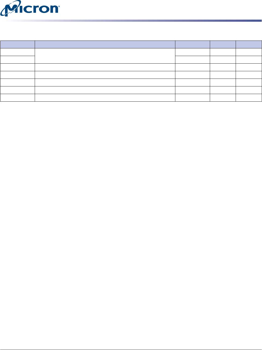
Table 9: Absolute Maximum Ratings
Symbol Parameter Min Max Units Notes
V
DD
V
DD
supply voltage relative to V
SS
–0.4 1.5 V 1
V
DDQ
V
DDQ
supply voltage relative to V
SS
–0.4 1.5 V 1
V
PP
Voltage on V
PP
pin relative to V
SS
–0.4 3.0 V 2
V
IN
, V
OUT
Voltage on any pin relative to V
SS
–0.4 1.5 V
Table 10: Operating Conditions
Symbol Parameter Min Nom Max Units Notes
V
DD
V
DD
supply voltage 1.14 1.2 1.26 V 1
V
PP
DRAM activating power supply 2.375 2.5 2.75 V 2
V
REFCA(DC)
Input reference voltage command/
address bus
0.49 × V
DD
0.5 × V
DD
0.51 × V
DD
V 3
I
VTT
Termination reference current from V
TT
–500 500 mA
V
TT
Termination reference voltage (DC) –
command/address bus
0.49 × V
DD
-
20mV
0.5 × V
DD
0.51 × V
DD
+
20mV
V 4
I
IN
Input leakage current; any input excluding ZQ;
0V < V
IN
< 1.1V
–2.0 2.0 µA 5
I
I/O
DQ leakage; 0V < V
in
< V
DD
–4.0 4.0 µA 5
I
ZQ
Input leakage current; ZQ –3.0 3.0 µA 5, 6
I
OZpd
Output leakage current; V
OUT
= V
DD
; DQ is disabled 5.0 µA
I
OZpu
Output leakage current; V
OUT
=V
SS
; DQ and ODT are
disabled; ODT is disabled with ODT input HIGH
5.0 µA
I
VREFCA
V
REFCA
leakage; V
REFCA
= V
DD
/2 (after DRAM is ini-
tialized)
–2.0 2.0 µA 5
Notes:
1. V
DDQ
tracks with V
DD
; V
DDQ
and V
DD
are tied together.
2. V
PP
must be greater than or equal to V
DD
at all times.
3. V
REFCA
must not be greater than 0.6 x V
DD
. When V
DD
is less than 500mV, V
REF
may be
less than or equal to 300mV.
4. V
TT
termination voltages in excess of the specification limit adversely affect the voltage
margins of command and address signals and reduce timing margins.
5. Multiply by the number of DRAM die on the module.
6. Tied to ground. Not connected to edge connector.
8GB (x64, SR) 260-Pin DDR4 SODIMM
Electrical Specifications
CCMTD-1725822587-9885
atf8c1gx64hz.pdf – Rev. F 9/16 EN
13
Micron Technology, Inc. reserves the right to change products or specifications without notice.
© 2015 Micron Technology, Inc. All rights reserved.
Table 11: Thermal Characteristics
Symbol Parameter/Condition Value Units Notes
T
C
Commercial operating case temperature 0 to 85 °C 1, 2, 3
T
C
>85 to 95 °C 1, 2, 3, 4
T
OPER
Normal operating temperature range 0 to 85 °C 5, 7
T
OPER
Extended temperature operating range (optional) >85 to 95 °C 5, 7
T
STG
Non-operating storage temperature –55 to 100 °C 6
RH
STG
Non-operating Storage Relative Humidity (non-condensing) 5 to 95 %
NA Change Rate of Storage Temperature 20 °C/hour
Notes:
1. Maximum operating case temperature; T
C
is measured in the center of the package.
2. A thermal solution must be designed to ensure the DRAM device does not exceed the
maximum T
C
during operation.
3. Device functionality is not guaranteed if the DRAM device exceeds the maximum T
C
dur-
ing operation.
4. If T
C
exceeds 85°C, the DRAM must be refreshed externally at 2X refresh, which is a 3.9µs
interval refresh rate.
5. The refresh rate must double when 85°C < T
OPER
95°C.
6. Storage temperature is defined as the temperature of the top/center of the DRAM and
does not reflect the storage temperatures of shipping trays.
7. For additional information, refer to technical note TN-00-08: "Thermal Applications"
available at micron.com.
8GB (x64, SR) 260-Pin DDR4 SODIMM
Electrical Specifications
CCMTD-1725822587-9885
atf8c1gx64hz.pdf – Rev. F 9/16 EN
14
Micron Technology, Inc. reserves the right to change products or specifications without notice.
© 2015 Micron Technology, Inc. All rights reserved.
DRAM Operating Conditions
Recommended AC operating conditions are given in the DDR4 component data sheets.
Component specifications are available at micron.com. Module speed grades correlate
with component speed grades, as shown below.
Table 12: Module and Component Speed Grades
DDR4 components may exceed the listed module speed grades; module may not be available in all listed speed grades
Module Speed Grade Component Speed Grade
-2G6 -075
-2G4 -083E
-2G3 -083
-2G1 -093E
-1G9 -107E
Design Considerations
Simulations
Micron memory modules are designed to optimize signal integrity through carefully de-
signed terminations, controlled board impedances, routing topologies, trace length
matching, and decoupling. However, good signal integrity starts at the system level. Mi-
cron encourages designers to simulate the signal characteristics of the system's memo-
ry bus to ensure adequate signal integrity of the entire memory system.
Power
Operating voltages are specified at the edge connector of the module, not at the DRAM.
Designers must account for any system voltage drops at anticipated power levels to en-
sure the required supply voltage is maintained.
8GB (x64, SR) 260-Pin DDR4 SODIMM
DRAM Operating Conditions
CCMTD-1725822587-9885
atf8c1gx64hz.pdf – Rev. F 9/16 EN
15
Micron Technology, Inc. reserves the right to change products or specifications without notice.
© 2015 Micron Technology, Inc. All rights reserved.

MTA8ATF1G64HZ-2G3B1

Mfr. #:
Manufacturer:
Micron
Description:
IC SDRAM DDR4 8GB 1GX64 FBGA
Lifecycle:
New from this manufacturer.
Delivery:
DHL FedEx Ups TNT EMS
Payment:
T/T Paypal Visa MoneyGram Western Union