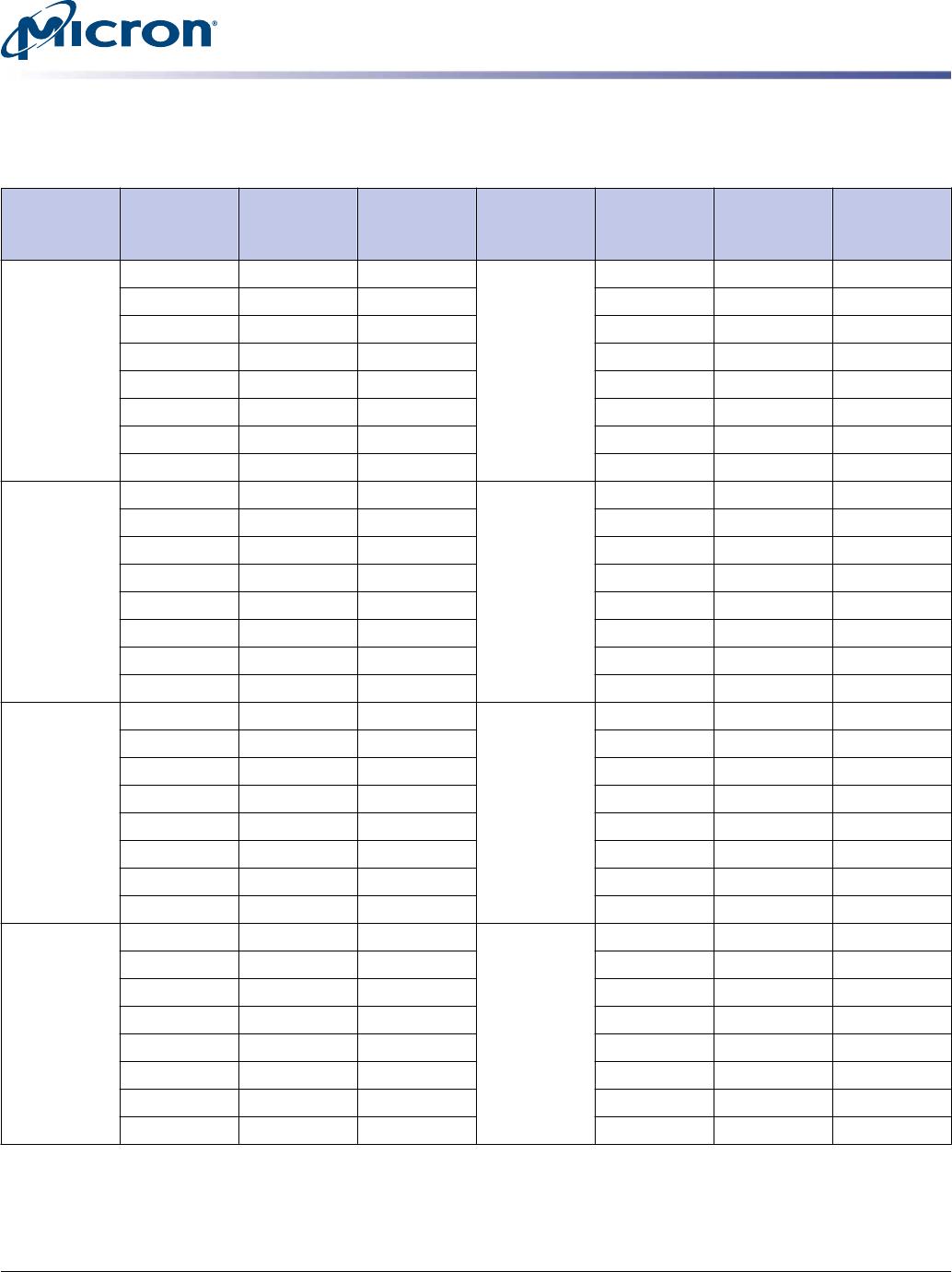
Table 5: Pin Descriptions (Continued)
Symbol Type Description
TDQS_t
TDQS_c
(x8 DRAM-based
RDIMM only)
Output Termination data strobe: When enabled via the mode register, the DRAM device enables the
same R
TT
termination resistance on TDQS_t and TDQS_c that is applied to DQS_t and DQS_c.
When the TDQS function is disabled via the mode register, the DM/TDQS_t pin provides the da-
ta mask (DM) function, and the TDQS_c pin is not used. The TDQS function must be disabled in
the mode register for both the x4 and x16 configurations. The DM function is supported only in
x8 and x16 configurations. DM, DBI, and TDQS are a shared pin and are enabled/disabled by
mode register settings. For more information about TDQS, see the DDR4 DRAM component da-
ta sheet (TDQS_t and TDQS_c are not valid for UDIMMs).
V
DD
Supply Module power supply: 1.2V (TYP).
V
PP
Supply DRAM activating power supply: 2.5V –0.125V / +0.250V.
V
REFCA
Supply Reference voltage for control, command, and address pins.
V
SS
Supply Ground.
V
TT
Supply Power supply for termination of address, command, and control V
DD
/2.
V
DDSPD
Supply Power supply used to power the I
2
C bus for SPD.
RFU – Reserved for future use.
NC – No connect: No internal electrical connection is present.
NF – No function: May have internal connection present, but has no function.
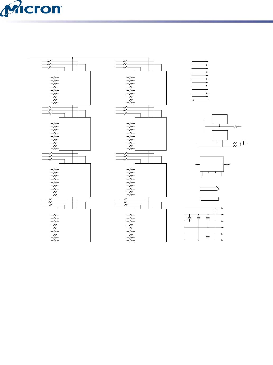
8GB (x64, SR) 260-Pin DDR4 SODIMM
Pin Descriptions
CCMTD-1725822587-9885
atf8c1gx64hz.pdf – Rev. F 9/16 EN
7
Micron Technology, Inc. reserves the right to change products or specifications without notice.
© 2015 Micron Technology, Inc. All rights reserved.