XC95288XL-6BGG256C

XC95288XL High Performance CPLD
4 www.xilinx.com DS055 (v2.1 April 3, 2007
1-800-255-7778 Product Specification
R
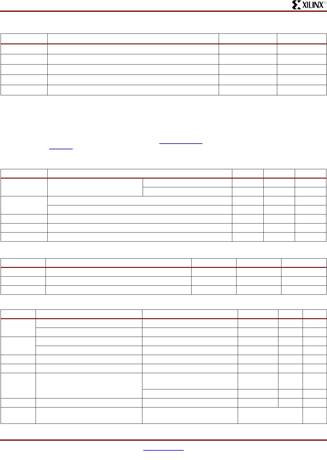
Absolute Maximum Ratings
(2)
Recommended Operation Conditions
Quality and Reliability Characteristics
DC Characteristic Over Recommended Operating Conditions
Symbol Description Value Units
V
CC
Supply voltage relative to GND –0.5 to 4.0 V
V
IN
Input voltage relative to GND
(1)
–0.5 to 5.5 V
V
TS
Voltage applied to 3-state output
(1)
–0.5 to 5.5 V
T
STG
Storage temperature (ambient)
(3)
–65 to +150
o
C
T
J
Junction temperature +150
o
C
Notes:
1. Maximum DC undershoot below GND must be limited to either 0.5V or 10 mA, whichever is easier to achieve. During transitions, the
device pins may undershoot to –2.0V or overshoot to +7.0V, provided this over- or undershoot lasts less than 10 ns and with the
forcing current being limited to 200 mA. External I/O voltage may not exceed V
CCINT
by 4.0V.
2. Stresses beyond those listed under Absolute Maximum Ratings may cause permanent damage to the device. These are stress
ratings only, and functional operation of the device at these or any other conditions beyond those listed under Operating Conditions
is not implied. Exposure to Absolute Maximum Ratings conditions for extended periods of time may affect device reliability.
3. For soldering guidelines and thermal considerations, see the Device Packaging
information on the Xilinx website. For Pb-free
packages, see XAPP427.
Symbol Parameter Min Max Units
V
CCINT
Supply voltage for internal logic
and input buffers
Commercial T
A
= 0
o
C to 70
o
C3.0 3.6 V
Industrial T
A
= –40
o
C to +85
o
C3.0 3.6 V
V
CCIO
Supply voltage for output drivers for 3.3V operation 3.0 3.6 V
Supply voltage for output drivers for 2.5V operation 2.3 2.7 V
V
IL
Low-level input voltage 0 0.80 V
V
IH
High-level input voltage 2.0 5.5 V
V
O
Output voltage 0 V
CCIO
V
Symbol Parameter Min Max Units
T
DR
Data Retention 20 - Years
N
PE
Program/Erase Cycles (Endurance) 10,000 - Cycles
V
ESD
Electrostatic Discharge (ESD) 2,000 - Volts
Symbol Parameter Test Conditions Min Max Units
V
OH
Output high voltage for 3.3V outputs I
OH
= –4.0 mA 2.4 - V
Output high voltage for 2.5V outputs I
OH
= –500 μA90% V
CCIO
-V
V
OL
Output low voltage for 3.3V outputs I
OL
= 8.0 mA - 0.4 V
Output low voltage for 2.5V outputs I
OL
= 500 μA-0.4V
I
IL
Input leakage current V
CC
= Max; V
IN
= GND or V
CC
10μA
I
IH
I/O high-Z leakage current V
CC
= Max; V
IN
= GND or V
CC
10μA
I
IH
I/O high-Z leakage current V
CC
= Max; V
CCIO
= Max;
V
IN
= GND or 3.6V
10μA
V
CC
Min < V
IN
< 5.5V - ±50 μA
C
IN
I/O capacitance V
IN
= GND; f = 1.0 MHz - 10 pF
I
CC
Operating supply current
(low power mode, active)
V
IN
= GND, No load; f = 1.0 MHz 85 (Typical) mA
XC95288XL High Performance CPLD
DS055 (v2.1 April 3, 2007 www.xilinx.com 5
Product Specification 1-800-255-7778
R
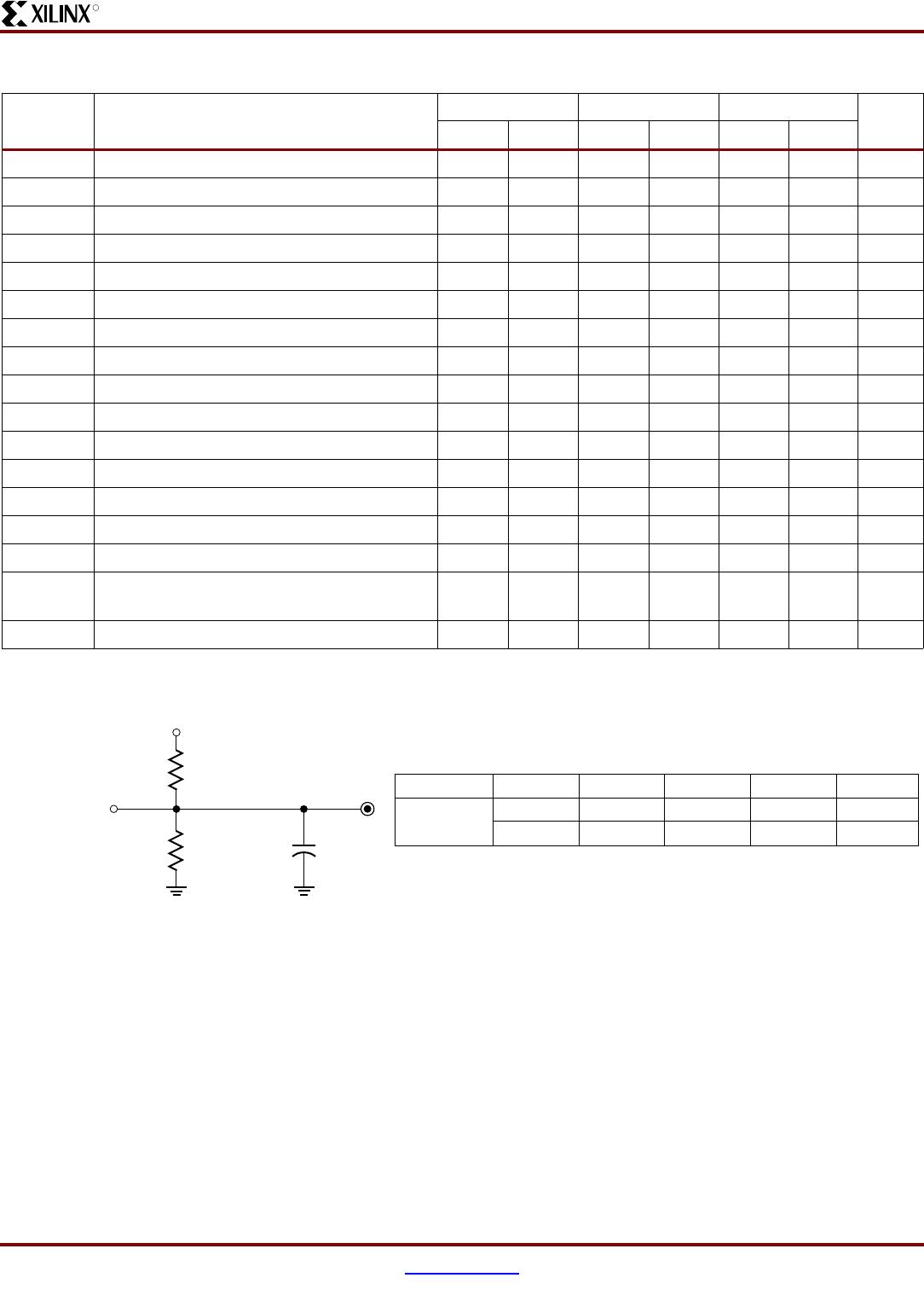
AC Characteristics
Symbol Parameter
XC95288XL-6 XC95288XL-7 XC95288XL-10
UnitsMin Max Min Max Min Max
T
PD
I/O to output valid - 6.0 - 7.5 - 10.0 ns
T
SU
I/O setup time before GCK 4.0 - 4.8 - 6.5 - ns
T
H
I/O hold time after GCK 0 - 0 - 0 - ns
T
CO
GCK to output valid - 3.8 - 4.5 - 5.8 ns
f
SYSTEM
Multiple FB internal operating frequency - 208.3 - 125.0 - 100.0 MHz
T
PSU
I/O setup time before p-term clock input 1.0 - 1.6 - 2.1 - ns
T
PH
I/O hold time after p-term clock input 2.6 - 3.2 - 4.4 - ns
T
PCO
P-term clock output valid - 6.8 - 7.7 - 10.2 ns
T
OE
GTS to output valid - 4.5 - 5.0 - 7.0 ns
T
OD
GTS to output disable - 4.5 - 5.0 - 7.0 ns
T
POE
Product term OE to output enabled - 8.4 - 9.5 - 11.0 ns
T
POD
Product term OE to output disabled - 8.4 - 9.5 - 11.0 ns
T
AO
GSR to output valid - 10.8 - 12.0 - 14.5 ns
T
PAO
P-term S/R to output valid - 11.8 - 12.6 - 15.3 ns
T
WLH
GCK pulse width (High or Low) 2.4 - 4.0 - 4.5 - ns
T
APRPW
Asynchronous preset/reset pulse width
(High or Low)
6.0 - 6.5 - 7.0 - ns
T
PLH
P-term clock pulse width (High or Low) 6.0 - 6.5 - 7.0 - ns
Figure 3: AC Load Circuit
Device Output
Output Type V
TEST
3.3V
2.5V
V
TEST
R
1
320 Ω
250 Ω
R
1
R
2
C
L
R
2
360 Ω
660 Ω
C
L
35 pF
35 pF
DS058_03_081500
V
CCIO
3.3V
2.5V
XC95288XL High Performance CPLD
6 www.xilinx.com DS055 (v2.1 April 3, 2007
1-800-255-7778 Product Specification
R
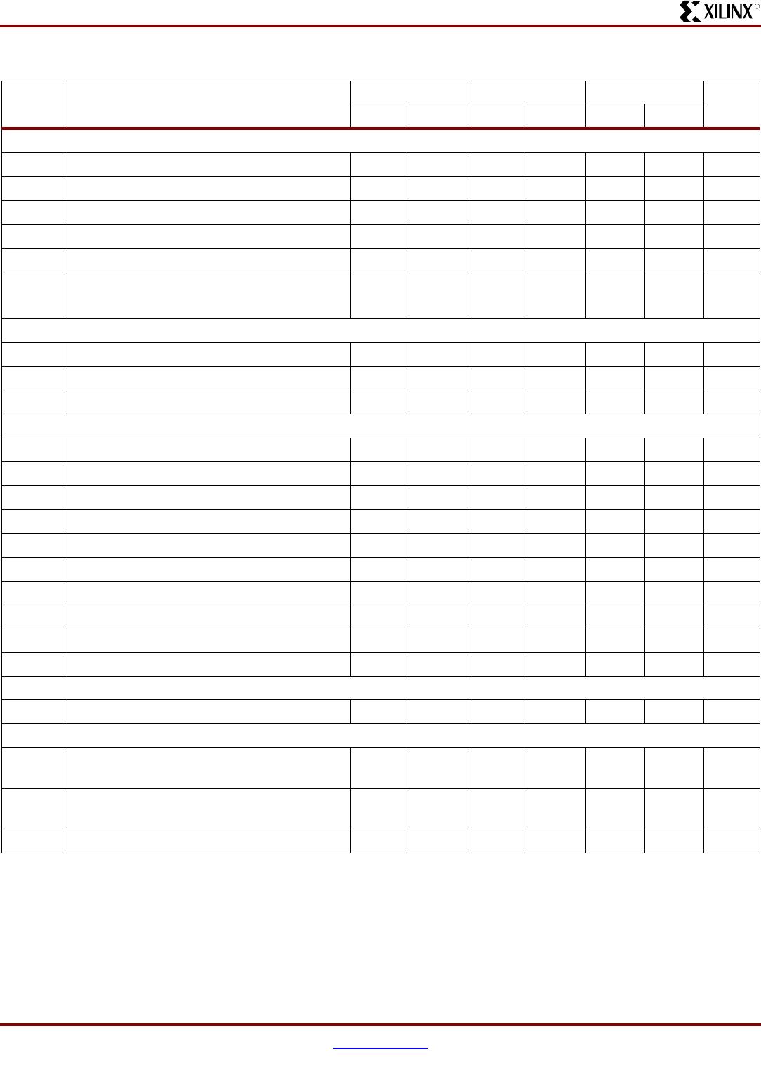
Internal Timing Parameters
Symbol Parameter
XC95288XL-6 XC95288XL-7 XC95288XL-10
UnitsMin Max Min Max Min Max
Buffer Delays
T
IN
Input buffer delay - 2.2 - 2.3 - 3.5 ns
T
GCK
GCK buffer delay - 1.2 - 1.5 - 1.8 ns
T
GSR
GSR buffer delay - 2.2 - 3.1 - 4.5 ns
T
GTS
GTS buffer delay - 4.5 - 5.0 - 7.0 ns
T
OUT
Output buffer delay - 2.4 - 2.5 - 3.0 ns
T
EN
Output buffer enable/disable
delay
-0-0-0ns
Product Term Control Delays
T
PTCK
Product term clock delay - 2.0 - 2.4 - 2.7 ns
T
PTSR
Product term set/reset delay - 1.0 - 1.4 - 1.8 ns
T
PTTS
Product term 3-state delay - 6.2 - 7.2 - 7.5 ns
Internal Register and Combinatorial Delays
T
PDI
Combinatorial logic propagation delay - 0.4 - 1.3 - 1.7 ns
T
SUI
Register setup time 2.0 - 2.6 - 3.0 - ns
T
HI
Register hold time 1.6 - 2.2 - 3.5 - ns
T
ECSU
Register clock enable setup time 2.0 - 2.6 - 3.0 - ns
T
ECHO
Register clock enable hold time 1.6 - 2.2 - 3.5 - ns
T
COI
Register clock to output valid time - 0.2 - 0.5 - 1.0 ns
T
AOI
Register async. S/R to output delay - 6.2 - 6.4 - 7.0 ns
T
RAI
Register async. S/R recover before clock 6.0 7.5 10.0 ns
T
LOGI
Internal logic delay - 1.0 - 1.4 - 1.8 ns
T
LOGILP
Internal low power logic delay - 5.5 - 6.4 - 7.3 ns
Feedback Delays
T
F
Fast CONNECT II feedback delay - 1.6 - 3.5 - 4.2 ns
Time Adders
T
PTA
Incremental product term allocator delay
(first incremental delay)
-0.8-0.8-1.0ns
T
PTA2
Incremental product term allocator delay
(subsequent incremental delay)
-0.3-0.3-0.4ns
T
SLEW
Slew-rate limited delay - 3.5 - 4.0 - 4.5 ns

XC95288XL-6BGG256C

Mfr. #:
Manufacturer:
Xilinx
Description:
CPLD - Complex Programmable Logic Devices 3.3V 288-mc CPLD
Lifecycle:
New from this manufacturer.
Delivery:
DHL FedEx Ups TNT EMS
Payment:
T/T Paypal Visa MoneyGram Western Union