Table 11: I
DD
Specifications – 1GB DDR2-667 (Die revision M)
Symbol I
DD_IDLE_0
I
DD_IDLE_1
I
DD_ACTIVE_1
I
DD_ACTIVE_2
I
DD_TRAINING
I
DD_IBIST
I
DD_EI
Units
I
CC
2600 3400 3900 3700 4000 4500 2500 mA
I
DD
916 916 1945 916 916 916 290 mA
Total power 5.8 7.0 9.8 7.5 8.0 8.8 4.5 W
Table 12: I
DD
Specifications – 1GB DDR2-800 (All die revisions)
Symbol I
DD_IDLE_0
I
DD_IDLE_1
I
DD_ACTIVE_1
I
DD_ACTIVE_2
I
DD_TRAINING
I
DD_IBIST
I
DD_EI
Units
I
CC
TBD TBD TBD TBD TBD TBD TBD mA
I
DD
TBD TBD TBD TBD TBD TBD TBD mA
Total power TBD TBD TBD TBD TBD TBD TBD W
Note:
1. Total power is based on maximum voltage levels, I
CC
at 1.575V and I
DD
at 1.9V.
Serial Presence-Detect
For the latest SPD data, refer to Micron's SPD page: www.micron.com/SPD.
Table 13: Serial Presence-Detect EEPROM DC Operating Conditions
Parameter/Condition Symbol Min Max Units
EEPROM and AMB supply voltage V
DDSPD
3 3.6 V
Input high voltage: Logic 1; all inputs V
IH
V
DDSPD
× 0.7 V
DDSPD
+ 0.5 V
Input low voltage: Logic 0; all inputs V
IL
–0.6 V
DDSPD
× 0.3 V
Output low voltage: I
OUT
= 3mA V
OL
– 0.4 V
Input leakage current: V
IN
= GND to V
DD
I
LI
0.10 3 µA
Output leakage current: V
OUT
= GND to V
DD
I
LO
0.05 3 µA
Standby current I
SB
1.6 4 µA
Power supply current, READ: SCL clock frequency = 100 kHz I
CCR
0.4 1 mA
Power supply current, WRITE: SCL clock frequency = 100 kHz I
CCW
2 3 mA
Table 14: Serial Presence-Detect EEPROM AC Operating Conditions
Parameter/Condition Symbol Min Max Units Notes
SCL LOW to SDA data-out valid
t
AA 0.2 0.9 µs 1
Time the bus must be free before a new transition can start
t
BUF 1.3 – µs
Data-out hold time
t
DH 200 – ns
SDA and SCL fall time
t
F – 300 ns 2
Data-in hold time
t
HD:DAT 0 – µs
Start condition hold time
t
HD:STA 0.6 – µs
Clock HIGH period
t
HIGH 0.6 – µs
Noise suppression time constant at SCL, SDA inputs
t
I – 50 ns
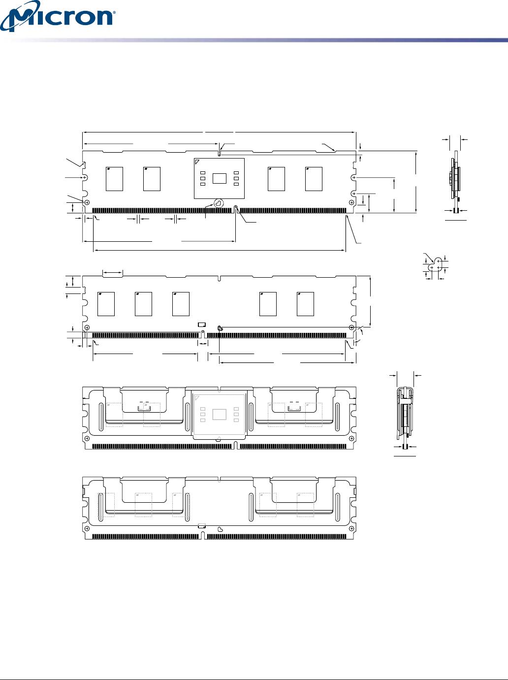
1GB (x72, SR) 240-Pin DDR2 SDRAM FBDIMM
Serial Presence-Detect
PDF: 09005aef83de8266
htf9c128x72fz.pdf - Rev. B 4/14 EN
10
Micron Technology, Inc. reserves the right to change products or specifications without notice.
© 2009 Micron Technology, Inc. All rights reserved.