MT9HTF12872FZ-667H1N8

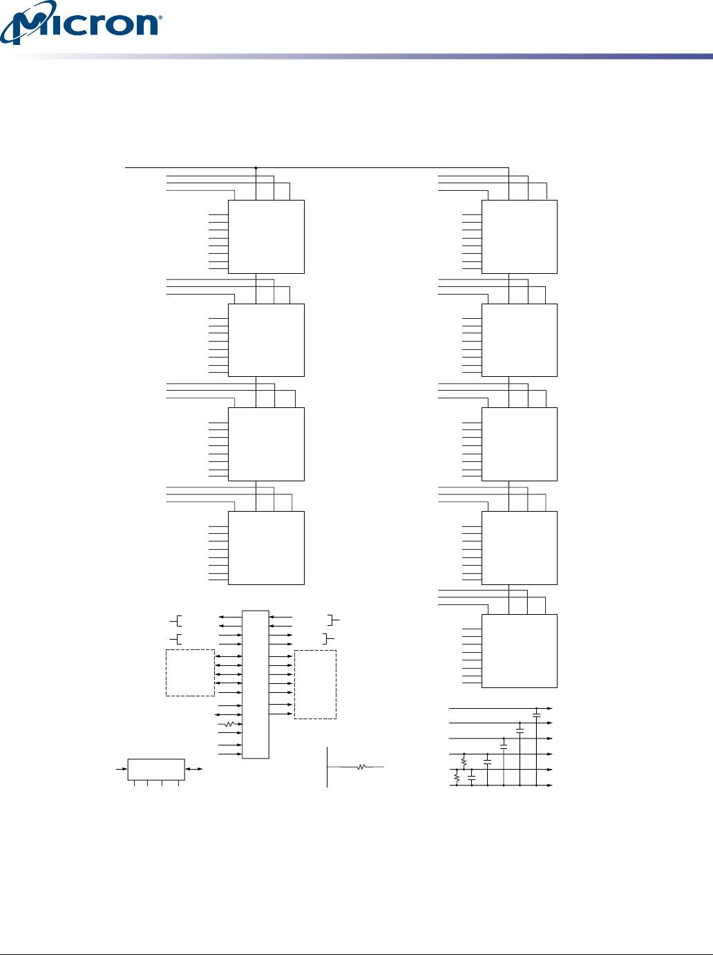
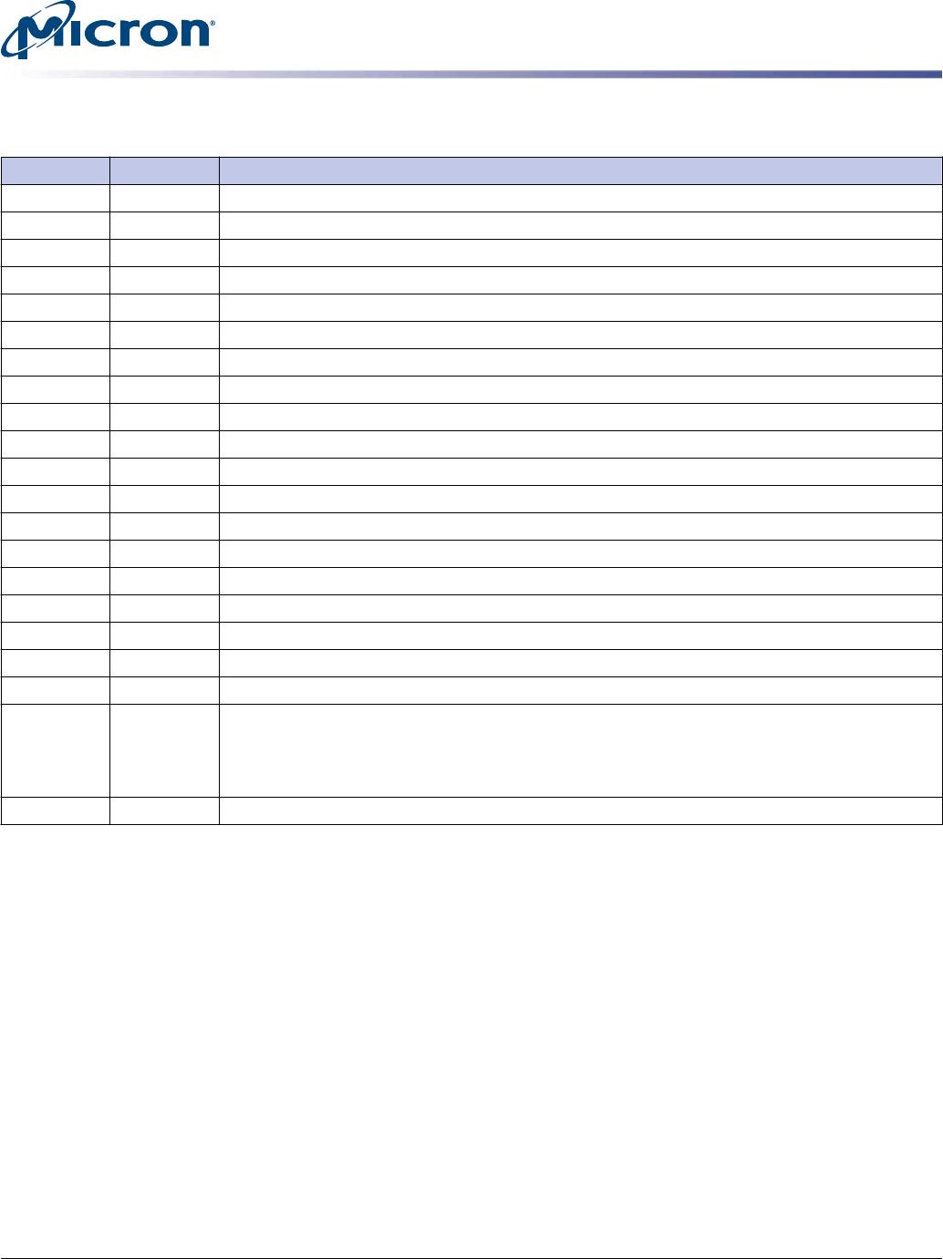
Table 5: Pin Descriptions
Symbol Type Description
PS[9:0] Input Primary southbound data, positive lines.
PS#[9:0] Input Primary southbound data, negative lines.
SCK Input System clock input, positive line.
SCK# Input System clock Input, negative line.
SCL Input Serial presence-detect (SPD) clock input.
SS[9:0] Input Secondary southbound data, positive lines.
SS#[9:0] Input Secondary southbound data, negative lines.
PN[13:0] Output Primary northbound data, positive lines.
PN#[13:0] Output Primary northbound data, negative lines.
SN[13:0] Output Secondary northbound data, positive lines.
SN#[13:0] Output Secondary northbound data, negative lines.
SA[2:0] I/O SPD address inputs, also used to select the FBDIMM number in the AMB.
SDA I/O SPD data input/output.
RESET# Supply AMB reset signal.
V
CC
Supply AMB core power and AMB channel interface power (1.5V).
V
DD
Supply DRAM power and AMB DRAM I/O power (1.8V).
V
DDSPD
Supply SPD/AMB SMBUS power (3.3V).
V
SS
Supply Ground.
V
TT
Supply DRAM address/command/clock termination power (V
DD
/2).
M_TEST The M_Test pin provides an external connection for testing the margin of V
REF
, which is pro-
duced by a voltage divider on the module. It is not intended to be used in normal system op-
eration and must not be connected (DNU) in a system. This test pin may have other features
on future card designs and will be included in this specification at that time.
DNU Do not use.
1GB (x72, SR) 240-Pin DDR2 SDRAM FBDIMM
Pin Assignments and Descriptions
PDF: 09005aef83de8266
htf9c128x72fz.pdf - Rev. B 4/14 EN
4
Micron Technology, Inc. reserves the right to change products or specifications without notice.
© 2009 Micron Technology, Inc. All rights reserved.
System Block Diagram
Figure 2: System Block Diagram
CK
source
SMBus
Up to 8 modules
10
14
Commodity
DDR2 SDRAM
devices
DDR2 connector with unique key
Common clock source
SMBus access
to buffer registers
AMB
DDR2
component
DDR2
component
DDR2
component
DDR2
component
DDR2
component
DDR2
component
DDR2
component
DDR2
component
AMB
DDR2
component
DDR2
component
DDR2
component
DDR2
component
DDR2
component
DDR2
component
DDR2
component
DDR2
component
AMB
DDR2
component
DDR2
component
DDR2
component
DDR2
component
DDR2
component
DDR2
component
DDR2
component
DDR2
component
AMB
DDR2
component
DDR2
component
DDR2
component
DDR2
component
DDR2
component
DDR2
component
DDR2
component
DDR2
component
Memory
controller
1GB (x72, SR) 240-Pin DDR2 SDRAM FBDIMM
System Block Diagram
PDF: 09005aef83de8266
htf9c128x72fz.pdf - Rev. B 4/14 EN
5
Micron Technology, Inc. reserves the right to change products or specifications without notice.
© 2009 Micron Technology, Inc. All rights reserved.
Functional Block Diagram
Figure 3: Functional Block Diagram
DQ
DQ
DQ
DQ
DQ
DQ
DQ
DQ
DQ0
DQ1
DQ2
DQ3
DQ4
DQ5
DQ6
DQ7
DM/ CS# DQS DQS#
RDQS
U1
DQ
DQ
DQ
DQ
DQ
DQ
DQ
DQ
DQ32
DQ33
DQ34
DQ35
DQ36
DQ37
DQ38
DQ39
DM/ CS# DQS DQS#
RDQS
U4
DQS0
DQS0#
DM0
DQS4
DQS4#
DM4
DQ
DQ
DQ
DQ
DQ
DQ
DQ
DQ
DQ8
DQ9
DQ10
DQ11
DQ12
DQ13
DQ14
DQ15
DM/ CS# DQS DQS#
RDQS
U11
DQ
DQ
DQ
DQ
DQ
DQ
DQ
DQ
DQ40
DQ41
DQ42
DQ43
DQ44
DQ45
DQ46
DQ47
DM/ CS# DQS DQS#
RDQS
U7
DQS5
DQS5#
DM5
DQ
DQ
DQ
DQ
DQ
DQ
DQ
DQ
DQ16
DQ17
DQ18
DQ19
DQ20
DQ21
DQ22
DQ23
DM/ CS# DQS DQS#
RDQS
U2
DQ
DQ
DQ
DQ
DQ
DQ
DQ
DQ
DQ48
DQ49
DQ50
DQ51
DQ52
DQ53
DQ54
DQ55
DM/ CS# DQS DQS#
RDQS
U5
DQS2
DQS2#
DM2
DQS6
DQS6#
DM6
DQ
DQ
DQ
DQ
DQ
DQ
DQ
DQ
DQ24
DQ25
DQ26
DQ27
DQ28
DQ29
DQ30
DQ31
DM/ CS# DQS DQS#
RDQS
U10
DQ
DQ
DQ
DQ
DQ
DQ
DQ
DQ
DQ56
DQ57
DQ58
DQ59
DQ60
DQ61
DQ62
DQ63
DM/ CS# DQS DQS#
RDQS
U6
DQS7
DQS7#
DM7
DQ
DQ
DQ
DQ
DQ
DQ
DQ
DQ
CB0
CB1
CB2
CB3
CB4
CB5
CB6
CB7
DM/ CS# DQS DQS#
RDQS
U8
DQS8
DQS8#
DM8
A0
SPD EEPROM
A1
A2
SA0 SA1 SA2
SDA
SCL
WP
A
M
B
SN[13:0]
SN#[13:0]
SS[9:0]
SS#[9:0]
A[15:0]
RAS#, CAS#
WE#, ODT0
CS0#
CKE0
CK0, CK0#
CK1, CK1#
PN[13:0]
PN#[13:0]
PS[9:0]
PS#[9:0]
DQ[63:0]
DQS[8:0]
DQS#[8:0]
CB[7:0]
DM[8:0]
SCL
SDA
SA0
SA[2:1]
SCK, SCK#
RESET#
V
REF
V
SS
V
DD
DDR2 SDRAM
V
DDSPD
SPD EEPROM, AMB
U9
Out to
controller
In from
adjacent FBDIMM
In from
controller
Out to
adjacent FBDIMM
Command, address, and
clock signals to DDR2 channel
U1–U2, U4–U8, U10–U11
Data input/output
signals to DDR2 channel
U1–U2, U4–U8, U10–U11
V
TT
CK0,CK0#,
CK1, CK1#,
ODT0, CS0#,
RAS#, CKE0,
CAS#, A[15:0],
WE#, BA[2:0]
Command, address, and clock line terminations:
V
TT
V
CC
Terminators
AMB
DDR2 SDRAM
SPD EEPROM, AMB
DDR2 SDRAM
U3
CS0#
DQS1
DQS1#
DM5
DQS3
DQS3#
DM5
V
SS
1GB (x72, SR) 240-Pin DDR2 SDRAM FBDIMM
Functional Block Diagram
PDF: 09005aef83de8266
htf9c128x72fz.pdf - Rev. B 4/14 EN
6
Micron Technology, Inc. reserves the right to change products or specifications without notice.
© 2009 Micron Technology, Inc. All rights reserved.

MT9HTF12872FZ-667H1N8

Mfr. #:
Manufacturer:
Micron
Description:
MODULE DDR2 SDRAM 1GB 240FBDIMM
Lifecycle:
New from this manufacturer.
Delivery:
DHL FedEx Ups TNT EMS
Payment:
T/T Paypal Visa MoneyGram Western Union