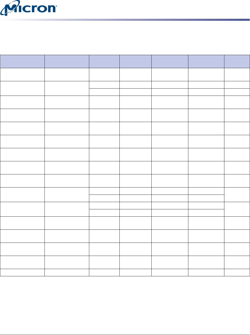
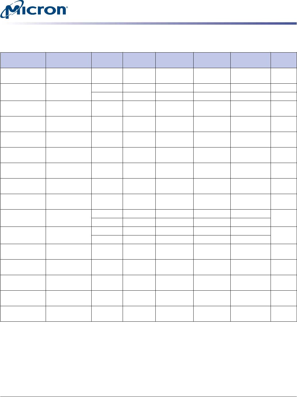
MT41K1G8TRF-125:E

Electrical Specifications – I
CDD
Parameters
Table 7: DDR3L I
CDD
Specifications and Conditions (Rev D)
Note 1 applies to the entire table
Combined
Symbol
Individual
Die Status
Bus
Width -187E -15E -125 Units
I
CDD0
I
CDD0
=
I
DD0
+ I
DD2P0
x4, x8 75 80 90 mA
I
CDD1
I
CDD1
=
I
DD1
+ I
DD2P0
x4 85 90 95 mA
x8 92 97 102
I
CDD2P0
(slow exit) I
CDD2P0
=
I
DD2P0
+ I
DD2P0
x4, x8 30 30 30 mA
I
CDD2P1
(fast exit) I
CDD2P1
=
I
DD2P1
+ I
DD2P0
x4, x8 43 45 50 mA
I
CDD2Q
I
CDD2Q
=
I
DD2Q
+ I
DD2P0
x4, x8 52 57 62 mA
I
CDD2N
I
CDD2N
=
I
DD2N
+ I
DD2P0
x4, x8 54 57 62 mA
I
CDD2N T
I
CDD2NT
=
I
DD2NT
+ I
DD2P0
x4, x8 55 60 65 mA
I
CDD3P
I
CDD3P
= I
DD3P
+
I
DD2P0
x4, x8 60 65 70 mA
I
CDD3N
I
CDD3N
=
I
DD3N
+ I
DD2P0
x4, x8 62 67 72 mA
I
CDD4R
I
CDD4RCDD4R
=
I
DD4R
+ I
DD2P0
x4 140 160 180 mA
x8 152 172 192
I
CDD4W
I
CDD4W
=
I
DD4W
+ I
DD2P0
x4 120 140 160 mA
x8 130 150 170
I
CDD5B
I
CDD5B
=
I
DD5B
+ I
DD2P0
x4, x8 215 220 230 mA
I
CDD6
I
CDD6
=
I
DD6
+ I
DD6
x4, x8 36 36 36 mA
I
CDD6ET
I
CDD6ET
=
I
DD6ET
+ I
DD6ET
x4, x8 48 48 48 mA
I
CDD7
I
CDD7
=
I
DD7
+ I
DD2P0
x4, x8 215 255 295 mA
I
CDD8
I
CDD8
= 2 × I
DD2P0
+ 4 x4, x8 34 34 34 mA
Note:
1. I
CDD
values reflect the combined current of both individual die. I
DDx
represents individu-
al die values.
8Gb: x4, x8 TwinDie DDR3L SDRAM
Electrical Specifications – I
CDD
Parameters
PDF: 09005aef84787542
DDR3L_8Gb_x4_x8_2CS_TwinDie.pdf - Rev. F 05/13 EN
10
Micron Technology, Inc. reserves the right to change products or specifications without notice.
© 2011 Micron Technology, Inc. All rights reserved.
Table 8: DDR3L I
CDD
Specifications and Conditions (Rev E)
Note 1 applies to the entire table
Combined
Symbol
Individual
Die Status
Bus
Width -187E -15E -125 -107 Units
I
CDD0
I
CDD0
=
I
DD0
+ I
DD2P0
+ 5
x4, x8 67 70 78 85 mA
I
CDD1
I
CDD1
=
I
DD1
+ I
DD2P0
+ 5
x4 76 80 84 88 mA
x8 82 85 89 93
I
CDD2P0
(slow exit) I
CDD2P0
=
I
DD2P0
+ I
DD2P0
x4, x8 36 36 36 36 mA
I
CDD2P1
(fast exit) I
CDD2P1
=
I
DD2P1
+ I
DD2P0
x4, x8 44 46 50 55 mA
I
CDD2Q
I
CDD2Q
=
I
DD2Q
+ I
DD2P0
x4, x8 45 46 50 53 mA
I
CDD2N
I
CDD2N
=
I
DD2N
+ I
DD2P0
x4, x8 46 47 50 53 mA
I
CDD2N T
I
CDD2NT
=
I
DD2NT
+ I
DD2P0
x4, x8 50 53 57 60 mA
I
CDD3P
I
CDD3P
= I
DD3P
+
I
DD2P0
x4, x8 50 53 56 59 mA
I
CDD3N
I
CDD3N
=
I
DD3N
+ I
DD2P0
x4, x8 50 53 56 59 mA
I
CDD4R
I
CDD4RCDD4R
=
I
DD4R
+ I
DD2P0
+ 5
x4 136 153 170 187 mA
x8 146 163 180 197
I
CDD4W
I
CDD4W
=
I
DD4W
+ I
DD2P0
+ 5
x4 110 126 141 156 mA
x8 118 133 148 164
I
CDD5B
I
CDD5B
=
I
DD5B
+ I
DD2P0
x4, x8 242 246 253 260 mA
I
CDD6
I
CDD6
=
I
DD6
+ I
DD6
x4, x8 40 40 40 40 mA
I
CDD6ET
I
CDD6ET
=
I
DD6ET
+ I
DD6ET
x4, x8 50 50 50 50 mA
I
CDD7
I
CDD7
=
I
DD7
+ I
DD2P0
+ 5
x4, x8 183 213 243 274 mA
I
CDD8
I
CDD8
= 2 × I
DD2P0
+ 4
x4, x8 40 40 40 40 mA
Note:
1. I
CDD
values reflect the combined current of both individual die. I
DDx
represents individu-
al die values.
8Gb: x4, x8 TwinDie DDR3L SDRAM
Electrical Specifications – I
CDD
Parameters
PDF: 09005aef84787542
DDR3L_8Gb_x4_x8_2CS_TwinDie.pdf - Rev. F 05/13 EN
11
Micron Technology, Inc. reserves the right to change products or specifications without notice.
© 2011 Micron Technology, Inc. All rights reserved.
Package Dimensions
Figure 5: 78-Ball FBGA Die Rev. D (package code THE)
Seating plane
0.12 A
123789
Ball A1 ID Ball A1 ID
A
0.25 MIN
1.1 ±0.1
6.4 CTR
10.5 ±0.1
0.8 TYP
9.6 CTR
12 ±0.1
78X Ø0.45
Dimensions apply to
solder balls post-reflow
on Ø0.33 NSMD ball pads.
0.8 TYP
A
B
C
D
E
F
G
H
J
K
L
M
N
Notes:
1. All dimensions are in millimeters.
2. Solder ball material: SAC305 (96.5% Sn, 3% Ag, 0.5% Cu).
8Gb: x4, x8 TwinDie DDR3L SDRAM
Package Dimensions
PDF: 09005aef84787542
DDR3L_8Gb_x4_x8_2CS_TwinDie.pdf - Rev. F 05/13 EN
12
Micron Technology, Inc. reserves the right to change products or specifications without notice.
© 2011 Micron Technology, Inc. All rights reserved.

MT41K1G8TRF-125:E

Mfr. #:
Manufacturer:
Micron
Description:
IC DRAM 8G PARALLEL 78FBGA
Lifecycle:
New from this manufacturer.
Delivery:
DHL FedEx Ups TNT EMS
Payment:
T/T Paypal Visa MoneyGram Western Union