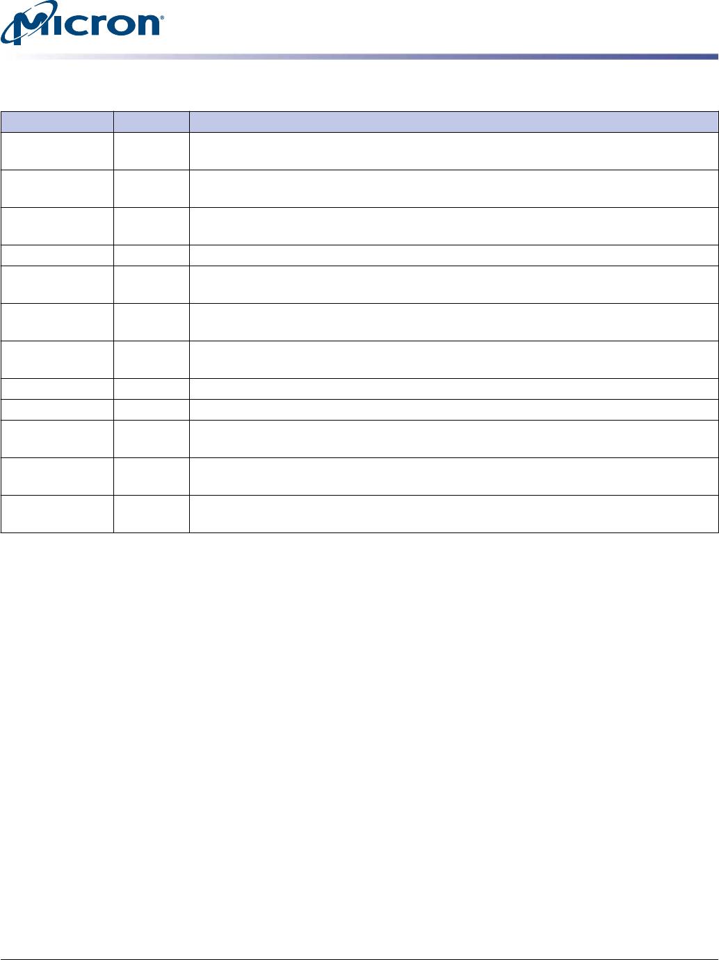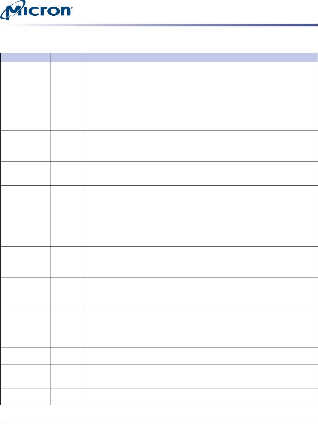
Table 3: FBGA 78-Ball Descriptions
Symbol Type Description
A15, A14, A13,
A12/BC#, A11,
A10/AP, A[9:0]
Input Address inputs: Provide the row address for ACTIVATE commands, and the column ad-
dress and auto precharge bit (A10) for READ/WRITE commands, to select one location out
of the memory array in the respective bank. A10 sampled during a PRECHARGE com-
mand determines whether the PRECHARGE applies to one bank (A10 LOW, bank selected
by BA[2:0]) or all banks (A10 HIGH). The address inputs also provide the op-code during a
LOAD MODE command. Address inputs are referenced to V
REFCA
. A12/BC#: When enabled
in the mode register (MR), A12 is sampled during READ and WRITE commands to deter-
mine whether burst chop (on-the-fly) will be performed (HIGH = burst length (BL) of 8 or
no burst chop, LOW = burst chop (BC) of 4, burst chop).
BA[2:0] Input Bank address inputs: BA[2:0] define the bank to which an ACTIVATE, READ, WRITE, or
PRECHARGE command is being applied. BA[2:0] define which mode register (MR0, MR1,
MR2, or MR3) is loaded during the LOAD MODE command. BA[2:0] are referenced to
V
REFCA
.
CK, CK# Input Clock: CK and CK# are differential clock inputs. All command, address, and control input
signals are sampled on the crossing of the positive edge of CK and the negative edge of
CK#. Output data strobe (DQS, DQS#) is referenced to the crossings of CK and CK#.
CKE[1:0] Input Clock enable: CKE enables (registered HIGH) and disables (registered LOW) internal cir-
cuitry and clocks on the DRAM. The specific circuitry that is enabled/disabled is depend-
ent upon the DDR3L SDRAM configuration and operating mode. Taking CKE LOW pro-
vides PRECHARGE power-down and SELF REFRESH operations (all banks idle) or active
power-down (row active in any bank). CKE is synchronous for power-down entry and exit
and for self refresh entry. CKE is asynchronous for self refresh exit. Input buffers (exclud-
ing CK, CK#, CKE, RESET#, and ODT) are disabled during power-down. Input buffers (ex-
cluding CKE and RESET#) are disabled during SELF REFRESH. CKE is referenced to V
REFCA
.
CS#[1:0] Input Chip select: CS# enables (registered LOW) and disables (registered HIGH) the command
decoder. All commands are masked when CS# is registered HIGH. CS# provides for exter-
nal rank selection on systems with multiple ranks. CS# is considered part of the command
code.
DM Input Input data mask: DM is an input mask signal for write data. Input data is masked when
DM is sampled HIGH, along with the input data, during a write access. Although the DM
ball is input-only, the DM loading is designed to match that of the DQ and DQS balls. DM
is referenced to V
REFDQ
. DM has an optional use as TDQS on the x8.
ODT[1:0] Input On-die termination: ODT enables (registered HIGH) and disables (registered LOW) ter-
mination resistance internal to the DDR3L SDRAM. When enabled in normal operation,
ODT is only applied to each of the following balls: DQ[7:0], DQS, DQS#, and DM for the
x8; DQ[3:0], DQS, DQS#, and DM for the x4. The ODT input is ignored if disabled via the
LOAD MODE command. ODT is referenced to V
REFCA
.
RAS#, CAS#, WE# Input Command inputs: RAS#, CAS#, and WE# (along with CS#) define the command being
entered and are referenced to V
REFCA
.
RESET# Input Reset: RESET# is an active LOW CMOS input referenced to V
SS
. The RESET# input receiver
is a CMOS input defined as a rail-to-rail signal with DC HIGH ≥ 0.8 × V
DDQ
and DC LOW ≤
0.2 × V
DDQ
. RESET# assertion and desertion are asynchronous.
DQ[3:0] I/O Data input/output: Bidirectional data bus for x4 configuration. DQ[3:0] are referenced
to V
REFDQ
.
8Gb: x4, x8 TwinDie DDR3L SDRAM
Ball Assignments and Descriptions
PDF: 09005aef84787542
DDR3L_8Gb_x4_x8_2CS_TwinDie.pdf - Rev. F 05/13 EN
4
Micron Technology, Inc. reserves the right to change products or specifications without notice.
© 2011 Micron Technology, Inc. All rights reserved.