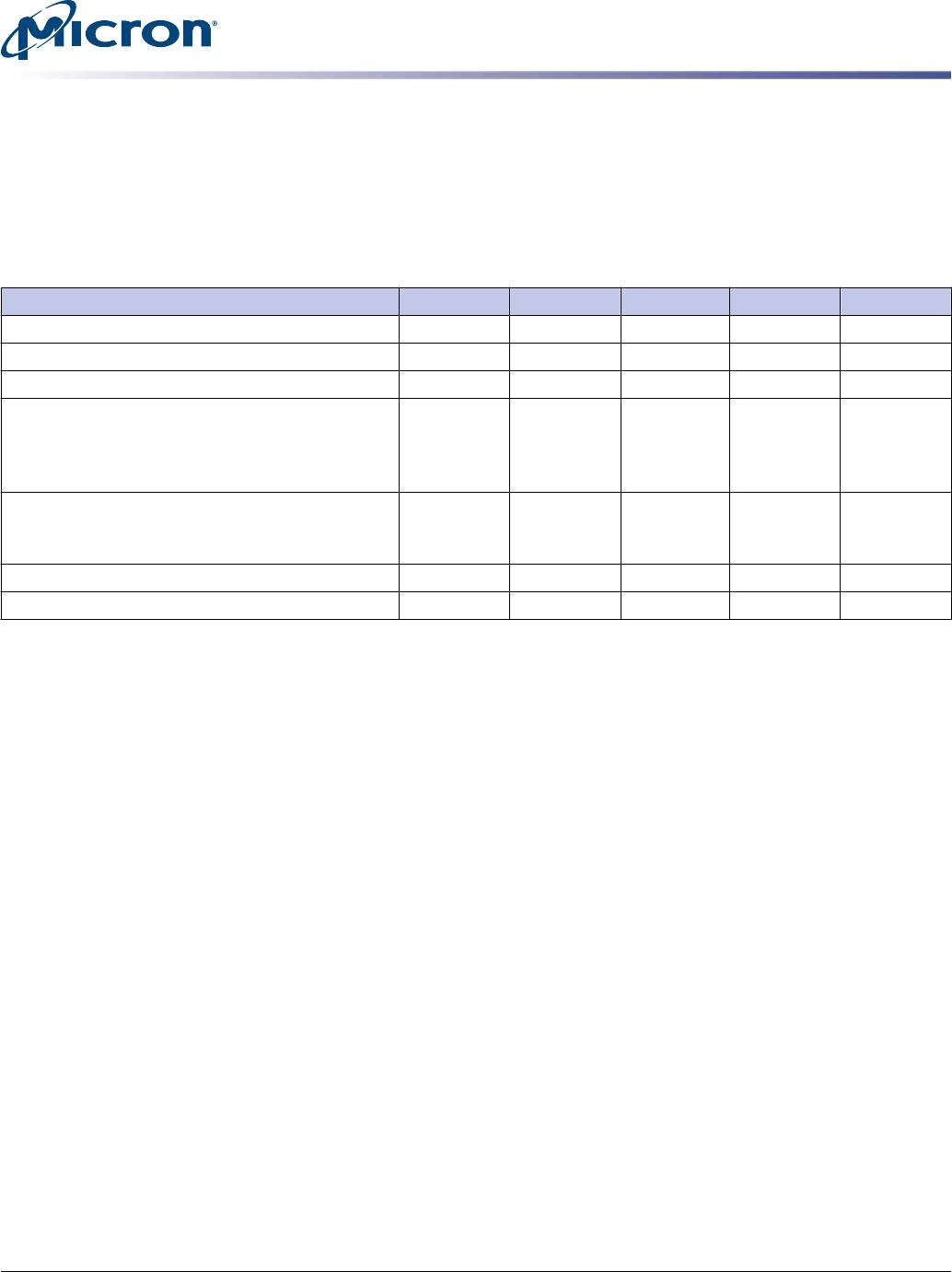
Electrical Specifications – Absolute Ratings
Stresses greater than those listed may cause permanent damage to the device. This is a
stress rating only, and functional operation of the device at these or any other condi-
tions outside those indicated in the device data sheet is not implied. Exposure to abso-
lute maximum rating conditions for extended periods may adversely affect reliability.
Table 4: Absolute Maximum DC Ratings
Parameter Symbol Min Max Units Notes
V
DD
supply voltage relative to V
SS
V
DD
–0.4 1.975 V 1
V
DD
supply voltage relative to V
SSQ
V
DDQ
–0.4 1.975 V
Voltage on any ball relative to V
SS
V
IN
, V
OUT
–0.4 1.975 V
Input leakage current
Any input 0V ≤ V
IN
≤ V
DD
,
V
REF
pin 0V ≤ V
IN
≤ 1.1V
(All other pins not under test = 0V)
I
I
–4 4 µA
V
REF
supply leakage current
V
REFDQ
= V
DD
/2 or V
REFCA
= V
DD
/2
(All other pins not under test = 0V)
I
VREF
–2 2 µA 2
Operating case temperature T
C
0 95 °C 3, 4
Storage temperature T
STG
–55 150 °C
Notes:
1. V
DD
and V
DDQ
must be within 300mV of each other at all times, and V
REF
must not be
greater than 0.6 × V
DDQ
. When V
DD
and V
DDQ
are less than 500mV, V
REF
may be ≤300mV.
2. The minimum limit requirement is for testing purposes. The leakage current on the V
REF
pin should be minimal.
3. MAX operating case temperature. T
C
is measured in the center of the package (see Fig-
ure 4 (page 9)).
4. Device functionality is not guaranteed if the DRAM device exceeds the maximum T
C
dur-
ing operation.
Temperature and Thermal Impedance
It is imperative that the DDR3L SDRAM device’s temperature specifications, shown in
the following table, be maintained in order to ensure the junction temperature is in the
proper operating range to meet data sheet specifications. An important step in main-
taining the proper junction temperature is using the device’s thermal impedances cor-
rectly. The thermal impedances listed in Table 6 (page 9) apply to the current die re-
vision and packages.
Incorrectly using thermal impedances can produce significant errors. Read Micron
technical note TN-00-08, “Thermal Applications,” prior to using the values listed in the
thermal impedance table. For designs that are expected to last several years and require
the flexibility to use several DRAM die shrinks, consider using final target theta values
(rather than existing values) to account for increased thermal impedances from the die
size reduction.
The DDR3L SDRAM device’s safe junction temperature range can be maintained when
the T
C
specification is not exceeded. In applications where the device’s ambient tem-
perature is too high, use of forced air and/or heat sinks may be required to satisfy the
case temperature specifications.
8Gb: x4, x8 TwinDie DDR3L SDRAM
Electrical Specifications – Absolute Ratings
PDF: 09005aef84787542
DDR3L_8Gb_x4_x8_2CS_TwinDie.pdf - Rev. F 05/13 EN
8
Micron Technology, Inc. reserves the right to change products or specifications without notice.
© 2011 Micron Technology, Inc. All rights reserved.