© 2008 Microchip Technology Inc. DS22062B-page 13
MCP14E3/MCP14E4/MCP14E5
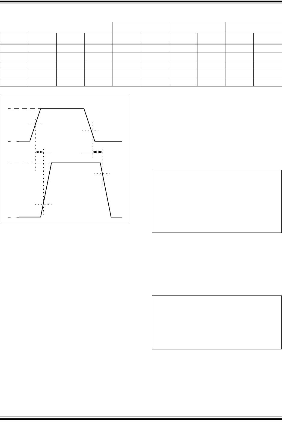
FIGURE 4-3: Enable Timing Waveform.
4.4 Decoupling Capacitors
Careful layout and decoupling capacitors are highly
recommended when using MOSFET drivers. Large
currents are required to charge and discharge
capacitive loads quickly. For example, 2.5A are needed
to charge a 2200 pF load with 18V in 16 ns.
To operate the MOSFET driver over a wide frequency
range with low supply impedance, a ceramic and low
ESR film capacitor are recommended to be placed in
parallel between the driver V
DD
and GND. A 1.0 µF low
ESR film capacitor and a 0.1 µF ceramic capacitor
should be used. These capacitors should be placed
close to the driver to minimized circuit board parasitics
and provide a local source for the required current.
4.5 PCB Layout Considerations
Proper PCB layout is important in a high current, fast
switching circuit to provide proper device operation and
robustness of design. PCB trace loop area and
inductance should be minimized by the use of ground
planes or trace under MOSFET gate drive signals,
separate analog and power grounds, and local driver
decoupling.
Placing a ground plane beneath the MCP14E3/
MCP14E4/MCP14E5 will help as a radiated noise
shield as well as providing some heat sinking for power
dissipated within the device.
4.6 Power Dissipation
The total internal power dissipation in a MOSFET driver
is the summation of three separate power dissipation
elements.
EQUATION 4-1:
4.6.1 CAPACITIVE LOAD DISSIPATION
The power dissipation caused by a capacitive load is a
direct function of frequency, total capacitive load, and
supply voltage. The power lost in the MOSFET driver
for a complete charging and discharging cycle of a
MOSFET is:
EQUATION 4-2:
TABLE 4-1: ENABLE PIN LOGIC
MCP14E3 MCP14E4 MCP14E5
ENB_A ENB_B IN A IN B OUT A OUT B OUT A OUT B OUT A OUT B
HHHHL LHHLH
HHHL LHHL LL
HHLHHL LHHH
HHL LHHL LHL
LLXXLLLLLL
5V
0V
ENB_x
V
DD
0V
OUT x
V
EN_H
V
EN_L
90%
10%
t
D3
t
D4
P
T
P
L
P
Q
P
CC
++=
Where:
P
T
= Total power dissipation
P
L
= Load power dissipation
P
Q
= Quiescent power dissipation
P
CC
= Operating power dissipation
P
L
fC
T
× V
DD
2
×=
Where:
f = Switching frequency
C
T
= Total load capacitance
V
DD
= MOSFET driver supply voltage