LTC1982ES6#TRMPBF

LTC1981/LTC1982
4
TYPICAL PERFOR A CE CHARACTERISTICS
UW
SUPPLY VOLTAGE (V)
2.0
TURN-ON TIME (µs)
1982 G06
1.5 2.5 3.0 3.5 4.0 4.5 5.0 5.5 6.0
400
350
300
250
200
150
100
50
0
C
GATE
= 1000pF
T
A
= 25°C
V
GS
= 2V
V
GS
= 1V
SUPPLY VOLTAGE (V)
2.0
TURN-OFF TIME (µs)
1982 G07
1.5 2.5 3.0 3.5 4.0 4.5 5.0 5.5 6.0
40
35
30
25
20
15
10
5
0
C
GATE
= 1000pF
T
A
= 25°C
TIME FOR V
GATE
< 0.1V
TEMPERATURE (°C)
–60
GATE DRIVE VOLTAGE (V)
7.50
7.45
7.40
7.35
7.30
7.25
7.20
7.15
7.10
7.05
7.00
–20
20
40
1982 G08
–40 0
60
80
100
V
CC
= 3.3V
Turn-Off Time (LTC1982)Turn-On Time (LTC1982)
GATE Drive Voltage vs
Temperature
Turn-On Time (LTC1981)GATE Drive Current (LTC1981) Turn-Off Time (LTC1981)
GATE DRIVE VOLTAGE (V)
01
100
10
1
0.1
2345678
GATE DRIVE CURRENT (µA)
1981/82 G09
V
CC
= 2.7V
V
CC
= 1.8V
V
CC
= 5V
V
CC
= 3.3V
SUPPLY VOLTAGE (V)
1.5
TURN-ON TIME (µs)
2.5
3.5
4.0 6.0
1981/82 G10
2.0 3.0
4.5
5.0
5.5
300
250
200
150
100
50
0
C
GATE
= 1000pF
T
A
= 25°C
V
GS
= 2V
V
GS
= 1V
SUPPLY VOLTAGE (V)
1.5
0
TURN-OFF TIME (µs)
5
15
20
25
2.5
3.5
4.0 6.0
1981/82 G11
10
2.0 3.0
4.5
5.0
5.5
C
GATE
=1000pF
T
A
= 25°C
TIME FOR V
GATE
< 0.1
PIN FUNCTIONS
UUU
LTC1981:
GDR (Pin 1): Gate Drive Ready Active High Open Drain
Output. Used to indicate when the gate drive output is
greater than 90% of its final value.
GND (Pin 2): Ground.
SHDN (Pin 3): SHDN Active Low Input. Used to shut down
the part and force the GATE output pin to ground.
GATE (Pin 4): Gate Drive Output to an External High Side
Switch. Fully enhanced by internal charge pump. Con-
trolled by the SHDN input pin. Output voltage on this pin
will be approximately 2.5 times V
CC
or 7.25V, whichever is
less.
V
CC
(Pin 5): Input Supply Voltage. Range from 1.8V to
5.5V.
LTC1982:
SHDN 1 (Pin 1): SHDN 1 Active Low Input. Used to shut
down the GATE 1 charge pump and force the GATE 1
output pin to ground.
GND (Pin 2): Ground.
SHDN 2 (Pin 3): SHDN 2 Active Low Input. Used to shut
down the GATE 2 charge pump and force the GATE 2
output pin to ground.
LTC1981/LTC1982
5
OPERATIO
U
Charge Pump
To fully enhance the external N-channel switches, internal
charge pumps are used to boost the output gate drive to
approximately 2.5 times the supply voltage, or 7.25V,
whichever is less. A feedback network is used to regulate
the output gate drive. This keeps the supply current low in
addition to providing a maximum output voltage limit. The
reason for the maximum output voltage limit is to avoid
switch gate source breakdown due to excessive gate
overdrive.
The gate drive outputs (GATE 1, GATE 2, or GATE) are
controlled by the shutdown input pins (SHDN 1, SHDN 2
or SHDN). A logic high input on one of the shutdown input
pins enables the corresponding charge pump and drives
the related gate drive output pin high. A logic low input on
one of the shutdown input pins disables the correspond-
ing charge pump and drives the related gate drive output
pin low. If shutdown input on the LTC1981 is low or both
of the shutdown input pins on the LTC1982 are low, the
part will be placed into a low current shutdown mode
(<1µA).
Gate Drive Ready (LTC1981 Only)
The gate drive ready pin (GDR) is used to indicate when the
gate drive output (GATE) is greater than 90% of its final
value. This can be useful in applications that require
knowledge of the state of the gate drive for initialization
purposes or as fault detection should something be load-
ing the gate drive down.
BLOCK DIAGRA SM
W
LTC1981 Single High Side Switch Driver
LTC1982 Dual High Side Switch Driver
REGULATING
CHARGE PUMP
EN
+
+
GATE
GDR
V
CC
REF
SHDN
1981/82 BD01
15k
REGULATING
CHARGE
PUMP 1
EN
GATE 1
SHDN 1
REGULATING
CHARGE
PUMP 2
EN
GATE 2
SHDN 2
1981/82 BD02
30k
30k
GATE 2(Pin 4): Gate Drive Output to an External High Side
Switch. Fully enhanced by internal charge pump. Con-
trolled by the SHDN 2 input pin. Output voltage on this pin
will be approximately 2.5 times V
CC
or 7.25V, whichever is
less.
GATE 1 (Pin 5): Gate Drive Output to an External High Side
Switch. Fully enhanced by internal charge pump. Con-
trolled by the SHDN 1 input pin. Output voltage on this pin
will be approximately 2.5 times V
CC
or 7.25V, whichever is
less.
V
CC
(Pin 6): Input Supply Voltage. Range from 1.8V to␣ 5.5V.
PIN FUNCTIONS
UUU
LTC1981/LTC1982
6
APPLICATIONS INFORMATION
WUU
U
Figure 3. Direct Interface to 3.3V Logic
V
CC
GATE 1
SHDN 1
GND
1/2 LTC1982
5V
LOAD
1981/82 F03
3.3V
5V
Si3442DV
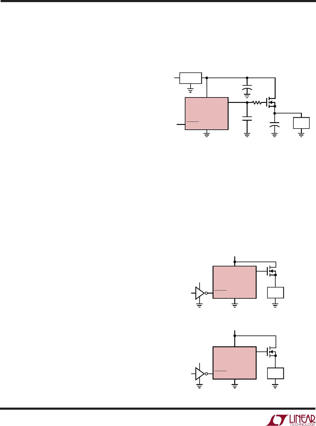
Figure 1. Powering a Large Capactive Load
Figure 2. Direct Interface to 5V Logic
Logic-Level MOSFET Switches
The LTC1981/LTC1982 are designed to operate with logic-
level N-channel MOSFET switches. Although there is some
variation among manufacturers, logic-level MOSFET
switches are typically rated with V
GS
= 4V with a maximum
continuous V
GS
rating of ±8V. RDS (ON) and maximum
V
DS
ratings are similar to standard MOSFETs and there is
generally little price differential. When operating at supply
voltages of 5V or greater, care must be taken when
selecting the MOSFET. The LTC1981/LTC1982 limit the
output voltage to between 6.9V and 7.5V. The V
GS
devel-
oped for the MOSFET may be too low to sufficiently turn on
the MOSFET. MOSFETs rated at 2.5V, or less, will be better
suited for applications where the supply voltages ap-
proach 5V.
Powering Large Capacitive Loads
Electrical subsystems in portable battery-powered equip-
ment are typically bypassed with large filter capacitors to
reduce supply transients and supply induced glitching. If
not properly powered however, these capacitors may
themselves become the source of supply glitching. For
example, if a 100µF capacitor is powered through a switch
with a slew rate of 0.1V/µs, the current during start-up is:
I
START
= C(V/t)
= (100 • 10
–6
)(1 • 10
5
)
= 10A
Obviously, this is too much current for the regulator (or
output capacitor) to supply and the output will glitch by as
much as a few volts.
The start up current can be substantially reduced by
limiting the slew rate at the gate of an N-channel as shown
in Figure 1. The gate drive output of the LTC1981/LTC1982
have an internal 30k resistor (15k LTC1981) in series with
each of the output gate drive pins (see Functional Block
Diagram). Therefore, it only needs an external 0.1µF
capacitor (0.22µF for the LTC1981) to create enough RC
delay to substantially slow the slew rate of the MOSFET
gate to approximately 0.6V/ms. Since the MOSFET is
operating as a source follower, the slew rate at the source
is essentially the same as that at the gate, reducing the
startup current to approximately 60mA which is easily
managed by the system regulator. R1 is required to
eliminate the possibility of parasitic MOSFET oscillations
during switch transitions. It is a good practice to isolate the
gates of paralleled MOSFETs with 1k resistors to decrease
the possibility of interaction between switches.
Mixed 5V/3V Systems
Because the input ESD protection diodes are referenced to
the GND pin instead of the supply pin, it is possible to drive
the LTC1981/LTC1982 inputs from 5V CMOS or TTL logic
even though the LTC1981/LTC1982 is powered from a
3.3V supply as shown in Figure 2. Likewise, because the
input threshold voltage high is never greater than 1.6V, the
reverse situation is true. The LTC1981/LTC1982 can be
driven with 3V CMOS or TTL even when the supply to the
device is as high as 5V as shown in Figure 3.
V
CC
GATE 1
SHDN 1
GND
1/2 LTC1982
+
LT1129-3.3
+
V
IN
ON/OFF
3.3µF
R1
1k
C1
0.1µF
C
L
100µF
3.3V
LOAD
1981/82 F01
3.3V
Si3442DV

LTC1982ES6#TRMPBF

Mfr. #:
Manufacturer:
Analog Devices / Linear Technology
Description:
Gate Drivers Dual Micropower Hi Side Sw Controller
Lifecycle:
New from this manufacturer.
Delivery:
DHL FedEx Ups TNT EMS
Payment:
T/T Paypal Visa MoneyGram Western Union