DS026 (v5.2) January 11, 2008 www.xilinx.com
Product Specification 1
© 1999–2008 Xilinx, Inc. All rights reserved. XILINX, the Xilinx logo, the Brand Window, and other designated brands included herein are trademarks of Xilinx, Inc. All other
trademarks are the property of their respective owners.
Features
In-System Programmable 3.3V PROMs for
Configuration of Xilinx FPGAs
Endurance of 20,000 Program/Erase Cycles
Program/Erase Over Full Industrial Voltage and
Temperature Range (–40
°C to +85°C)
IEEE Std 1149.1 Boundary-Scan (JTAG) Support
JTAG Command Initiation of Standard FPGA
Configuration
Simple Interface to the FPGA
Cascadable for Storing Longer or Multiple Bitstreams
Low-Power Advanced CMOS FLASH Process
Dual Configuration Modes
Serial Slow/Fast Configuration (up to 33 MHz)
Parallel (up to 264 Mb/s at 33 MHz)
5V-Tolerant I/O Pins Accept 5V, 3.3V and 2.5V Signals
3.3V or 2.5V Output Capability
Design Support Using the Xilinx ISE™ Foundation™
Software Packages
Available in PC20, SO20, PC44, and VQ44 Packages
Lead-Free (Pb-Free) Packaging
Description
Xilinx introduces the XC18V00 series of in-system
programmable configuration PROMs (Figure 1). Devices in
this 3.3V family include a 4-megabit, a 2-megabit, a
1-megabit, and a 512-kilobit PROM that provide an easy-to-
use, cost-effective method for reprogramming and storing
Xilinx FPGA configuration bitstreams.
When the FPGA is in Master Serial mode, it generates a
configuration clock that drives the PROM. A short access
time after CE
and OE are enabled, data is available on the
PROM DATA (D0) pin that is connected to the FPGA DIN
pin. New data is available a short access time after each
rising clock edge. The FPGA generates the appropriate
number of clock pulses to complete the configuration. When
the FPGA is in Slave Serial mode, the PROM and the FPGA
are clocked by an external clock.
When the FPGA is in Master SelectMAP mode, the FPGA
generates a configuration clock that drives the PROM. When
the FPGA is in Slave Parallel or Slave SelectMAP mode, an
external oscillator generates the configuration clock that
drives the PROM and the FPGA. After CE
and OE are
enabled, data is available on the PROM’s DATA (D0-D7)
pins. New data is available a short access time after each
rising clock edge. The data is clocked into the FPGA on the
following rising edge of the CCLK. A free-running oscillator
can be used in the Slave Parallel or Slave SelecMAP modes.
Multiple devices can be cascaded by using the CEO
output
to drive the CE
input of the following device. The clock
inputs and the DATA outputs of all PROMs in this chain are
interconnected. All devices are compatible and can be
cascaded with other members of the family or with the
XC17V00 one-time programmable serial PROM family.
24
XC18V00 Series In-System-Programmable
Configuration PROMs
DS026 (v5.2) January 11, 2008
0
Product Specification
R
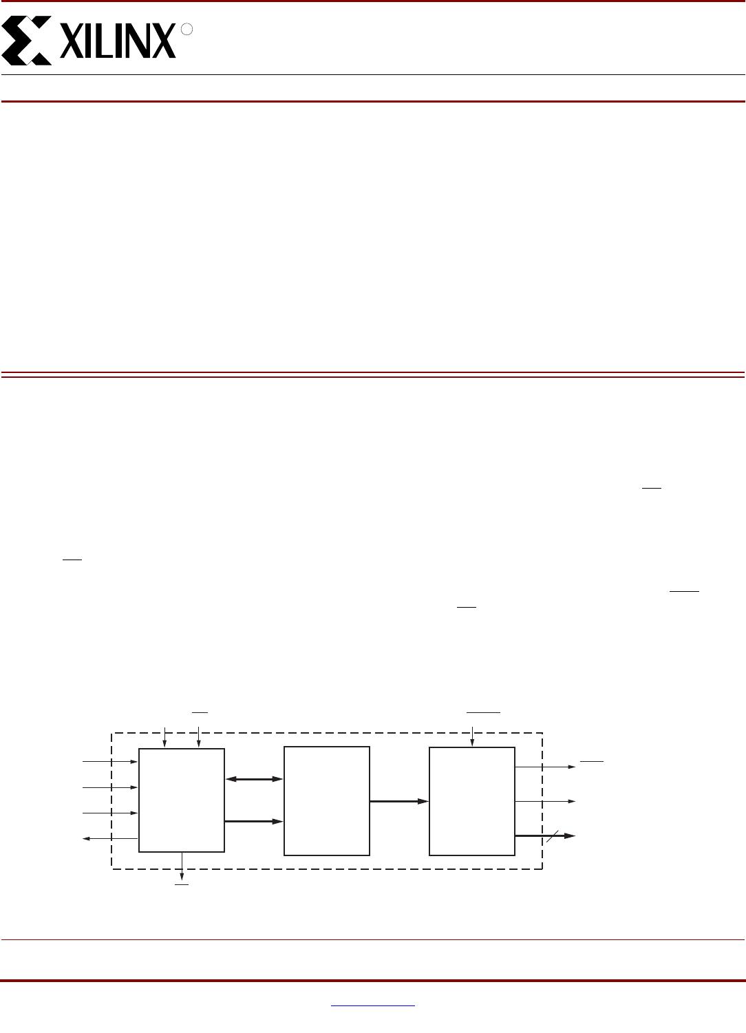
X-Ref Target - Figure 1
Figure 1: XC18V00 Series Block Diagram
Control
and
JTAG
Interface
Memory
Serial
or
Parallel
Interface
D0 DATA
Serial or Parallel Mode
D[1:7]
Parallel Interface
Data
Address
CLK CE
TCK
TMS
TDI
TDO
OE/RESET
CEO
Data
DS026_01_040204
7
CF
XC18V00 Series In-System-Programmable Configuration PROMs
DS026 (v5.2) January 11, 2008 www.xilinx.com
Product Specification 2
R
Pinout and Pin Description
Table 1 provides a list of the pin names and descriptions for the 44-pin VQFP and PLCC and the 20-pin SOIC and PLCC
packages.
Table 1: Pin Names and Descriptions
Pin
Name
Boundary-
Scan Order
Function Pin Description 44-pin VQFP
44-pin
PLCC
20-pin
SOIC &
PLCC
D0 4 DATA OUT D0 is the DATA output pin to provide data for
configuring an FPGA in serial mode.
40 2 1
3OUTPUT
ENABLE
D1 6 DATA OUT D0-D7 are the output pins to provide parallel
data for configuring a Xilinx FPGA in Slave
Parallel/SelectMAP mode.
D1-D7 remain in high-Z state when the PROM
operates in serial mode.
D1-D7 can be left unconnected when the
PROM is used in serial mode.
29 35 16
5OUTPUT
ENABLE
D2 2 DATA OUT 42 4 2
1OUTPUT
ENABLE
D3 8 DATA OUT 27 33 15
7OUTPUT
ENABLE
D4 24 DATA OUT 9 15 7
(1)
23 OUTPUT
ENABLE
D5 10 DATA OUT 25 31 14
9OUTPUT
ENABLE
D6 17 DATA OUT 14 20 9
16 OUTPUT
ENABLE
D7 14 DATA OUT 19 25 12
13 OUTPUT
ENABLE
CLK 0 DATA IN Each rising edge on the CLK input increments
the internal address counter if both CE
is Low
and OE/RESET
is High.
43 5 3
OE/
RESET
20 DATA IN When Low, this input holds the address
counter reset and the DATA output is in a high-
Z state. This is a bidirectional open-drain pin
that is held Low while the PROM is reset.
Polarity is NOT programmable.
13 19 8
19 DATA OUT
18 OUTPUT
ENABLE
CE 15 DATA IN When CE
is High, the device is put into low-
power standby mode, the address counter is
reset, and the DATA pins are put in a high-Z
state.
15 21 10
CF 22 DATA OUT Allows JTAG CONFIG instruction to initiate
FPGA configuration without powering down
FPGA. This is an open-drain output that is
pulsed Low by the JTAG CONFIG command.
10 16 7
(1)
21 OUTPUT
ENABLE
XC18V00 Series In-System-Programmable Configuration PROMs
DS026 (v5.2) January 11, 2008 www.xilinx.com
Product Specification 3
R
CEO 12 DATA OUT Chip Enable Output (CEO) is connected to the
CE
input of the next PROM in the chain. This
output is Low when CE
is Low and OE/RESET
input is High, AND the internal address counter
has been incremented beyond its Terminal
Count (TC) value. CEO
returns to High when
OE/RESET
goes Low or CE goes High.
21 27 13
11 OUTPUT
ENABLE
GND GND is the ground connection. 6, 18, 28 & 41 3, 12, 24 &
34
11
TMS MODE
SELECT
The state of TMS on the rising edge of TCK
determines the state transitions at the Test
Access Port (TAP) controller. TMS has an
internal 50 kΩ resistive pull-up to provide a
logic 1 to the device if the pin is not driven.
5115
TCK CLOCK This pin is the JTAG test clock. It sequences
the TAP controller and all the JTAG test and
programming electronics.
7136
TDI DATA IN This pin is the serial input to all JTAG
instruction and data registers. TDI has an
internal 50 kΩ resistive pull-up to provide a
logic 1 to the device if the pin is not driven.
394
TDO DATA OUT This pin is the serial output for all JTAG
instruction and data registers. TDO has an
internal 50 kΩ resistive pull-up to provide a
logic 1 to the system if the pin is not driven.
31 37 17
V
CCINT
Positive 3.3V supply voltage for internal logic. 17, 35 & 38
(3)
23, 41 &
44
(3)
18 & 20
(3)
V
CCO
Positive 3.3V or 2.5V supply voltage connected
to the input buffers
(2)
and output voltage
drivers.
8, 16, 26 & 36 14, 22, 32 &
42
19
NC No connects. 1, 2, 4,
11, 12, 20, 22,
23, 24, 30, 32,
33, 34, 37, 39,
44
1, 6, 7, 8,
10, 17, 18,
26, 28, 29,
30, 36, 38,
39, 40, 43
Notes:
1. By default, pin 7 is the D4 pin in the 20-pin packages. However, CF D4 programming option can be set to override the default and route
the CF function to pin 7 in the Serial mode.
2. For devices with IDCODES 0502x093h, the input buffers are supplied by V
CCINT
.
3. For devices with IDCODES 0503x093h, the following V
CCINT
pins are no-connects: pin 38 in 44-pin VQFP package, pin 44 in 44-pin PLCC
package, and pin 20 in 20-pin SOIC and 20-pin PLCC packages.
Table 1: Pin Names and Descriptions (Cont’d)
Pin
Name
Boundary-
Scan Order
Function Pin Description 44-pin VQFP
44-pin
PLCC
20-pin
SOIC &
PLCC

XC18V512PC20C

Mfr. #:
Manufacturer:
Xilinx
Description:
FPGA - Configuration Memory
Lifecycle:
New from this manufacturer.
Delivery:
DHL FedEx Ups TNT EMS
Payment:
T/T Paypal Visa MoneyGram Western Union