Expand menu
Hello, Sign in
My Account
0
Cart
Home
Products
Sensors
Semiconductors
Passive Components
Connectors
Power
Electromechanical
Optoelectronics
Circuit Protection
Integrated Circuits - ICs
Main Products
Manufacturers
Blog
Services
About OMO
About Us
Contact Us
Check Stock
XC18V512PC20C
P1-P3
P4-P6
P7-P9
P10-P12
P13-P15
P16-P18
P19-P21
P22-P24
XC18V00 Series In-System-
Prog
ramma
ble Configuration PR
OMs
DS026 (v5.2) January 11, 20
08
www
.xilinx.com
Product Specification
10
R
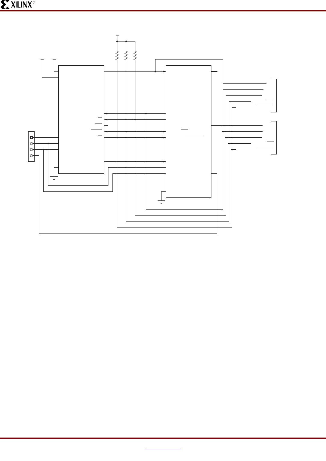
X-Ref Target - Figure 5
Figure 5:
Master Serial Mode
Xilinx FPGA
Master Serial
DIN
CCLK
DONE
INIT_B (INIT)
PROG_B (PROGRAM)
TDI
TMS
TCK
GND
MODE PINS
(1)
DOUT
TDO
V
CCO
V
CCINT
DOUT
CCLK
DONE
INIT_B (INIT)
PROG_B (PROGRAM)
DIN
CCLK
DONE
INIT_B (INIT)
PROG_B (PROGRAM)
4.7 k
Ω
4.7 k
Ω
(1)
V
CCO
(2)
...OPTIONAL
Daisy-chained
Slav
e FPGAs
with
different
configurations
...OPTIONAL
Slav
e FPGAs
with
identical
configurations
TDI
TMS
TCK
TDO
Notes:
1 For MODE pin connections and DONE pin pullup v
alue, refer to the appropriate FPGA data sheet or user guide.
2 For compatib
le voltages, refer to the appropriate data sheet.
XC1
8
V00
PROM
V
CCINT
V
CCO
(2)
TDI
TMS
TCK
GND
D0
CLK
CE
CEO
OE/RESET
CF
TDO
ds026_18_20051007
XC18V00 Series In-System-
Prog
ramma
ble Configuration PR
OMs
DS026 (v5.2) January 11, 20
08
www
.xilinx.com
Product Specification
11
R
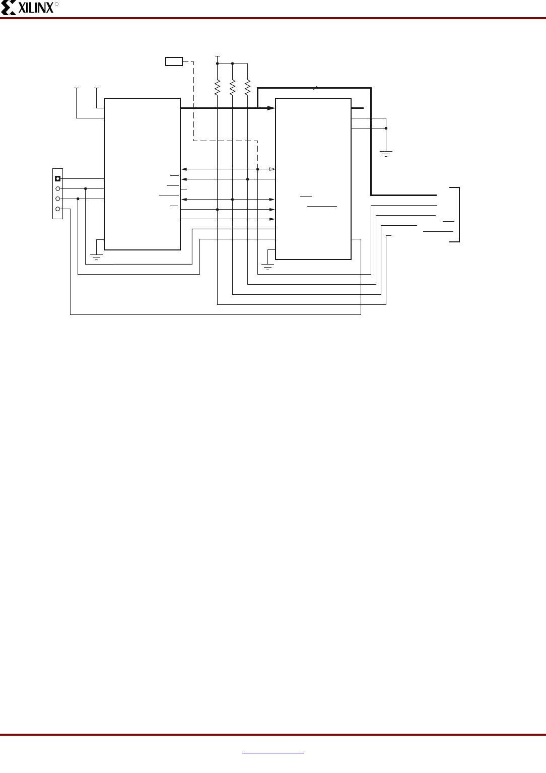
X-Ref Target - Figure 6
Figure 6:
Master/Slave SelectMAP Mode or Slave P
arallel Mode
XC1
8
V00
PROM
V
CCINT
V
CCO
(2)
GND
D[0:7]
CLK
CE
CEO
OE/RE
S
ET
CF
TDO
Xilinx FPGA
S
electMAP or
S
lave-P
arallel
D[0:7]
CCLK
DONE
INIT_B (INIT)
PROG_B (PROGRAM)
TDI
TM
S
TCK
GND
MODE PIN
S
(1)
RDWR_B
C
S
_B
TDO
V
CCO
V
CCINT
D[0:7]
CCLK
DONE
INIT_B (INIT)
PROG_B (PROGRAM)
4.7 k
Ω
4.7 k
Ω
(1)
V
CCO
(2)
...OPTIONAL
S
l
a
v
e FPGA
s
with
identic
a
l
config
u
r
a
tion
s
Note
s
:
1 For MODE pin connection
s
a
nd DONE pin p
u
ll
u
p v
a
l
u
e, refer to the
a
ppropri
a
te FPGA d
a
t
a
s
heet or
us
er g
u
ide.
2 For comp
a
ti
b
le volt
a
ge
s
, refer to the
a
ppropri
a
te d
a
t
a
s
heet.
3
Extern
a
l o
s
cill
a
tor re
qu
ired for
Vir
tex/Vir
tex-E
S
electMAP
, for
Vir
tex-II/Virtex-II Pro
S
l
a
ve
S
electMAP
,
a
nd for
S
p
a
rt
a
n-II/
S
p
a
rt
a
n-IIE
S
l
a
ve-P
a
r
a
llel mode
s
.
D
S
026_19_111207
Extern
a
l
O
s
cill
a
tor
(
3
)
TDI
TM
S
TCK
TDO
8
XC18V00 Series In-System-
Prog
ramma
ble Configuration PR
OMs
DS026 (v5.2) January 11, 20
08
www
.xilinx.com
Product Specification
12
R
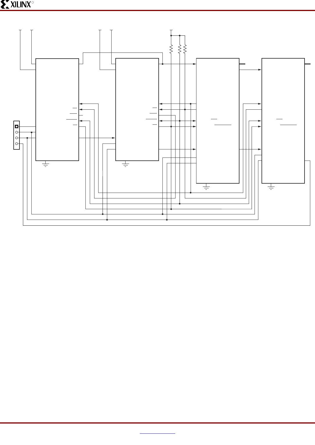
X-Ref Target - Figure 7
Figure 7:
Configuring Multiple Devices in Master/Slave Serial Mode
XC1
8
V00
PROM
First
PROM
(PROM 0)
V
CCINT
V
CCO
(2)
TDI
TMS
TCK
D0
CLK
CE
CEO
OE/RESET
CF
TDO
Xilinx FPGA
Master Serial
DIN
CCLK
DONE
INIT_B (INIT)
PROG_B (PROGRAM)
TDI
TMS
TCK
MODE PINS
(1)
DOUT
TDO
4.7 k
Ω
4.7 k
Ω
(1)
V
CCO
(2)
TDI
TMS
TCK
TDO
Notes:
1 For MODE pin connections and DONE pin pullup v
alue, refer to the appropriate FPGA data sheet or user guide.
2 For compatib
le voltages, refer to the appropriate data sheet.
Xilinx FPGA
Slave Serial
DIN
CCLK
DONE
INIT_B (INIT)
PROG_B (PROGRAM)
TDI
TMS
TCK
XC1
8
V00
PROM
Cascaded
PROM
(PROM 1)
V
CCINT
V
CCO
(2)
TDI
TMS
TCK
D0
CLK
CE
CEO
OE/RESET
CF
TDO
V
CCO
V
CCINT
MODE PINS
(1)
TDO
ds026_16_20051007
GND
GND
GND
GND
V
CCO
V
CCINT
P1-P3
P4-P6
P7-P9
P10-P12
P13-P15
P16-P18
P19-P21
P22-P24
XC18V512PC20C
Mfr. #:
Buy XC18V512PC20C
Manufacturer:
Xilinx
Description:
FPGA - Configuration Memory
Lifecycle:
New from this manufacturer.
Delivery:
DHL
FedEx
Ups
TNT
EMS
Payment:
T/T
Paypal
Visa
MoneyGram
Western
Union
Products related to this Datasheet
XC18V01VQ44C
XC18V04PC44C
XC18V01VQG44C
XC18V512SO20C
XC18V01PCG20C
XC18V04PCG44C
XC18V512VQG44C
XC18V04VQ44C
XC18V512VQ44C
XC18V512PC20C
XC18V02PCG44C
XC18V512PCG20C
XC18V01PC20C
XC18V01SO20C
XC18V01SOG20C
XC18V02VQ44C
XC18V02VQG44C
XC18V04VQG44C
XC18V512SOG20C
XC18V02PC44C
XC18V02PC44C0936