1
OCTOBER 2014
DSC-4667/17
©
2014 Integrated Device Technology, Inc. All rights reserved. Product specifications subject to change without notice.
3.3V HIGH-DENSITY SUPERSYNC™ II 36-BIT FIFO
1,024 x 36, 2,048 x 36
4,096 x 36, 8,192 x 36
16,384 x 36, 32,768 x 36
IDT72V3640, IDT72V3650
IDT72V3660, IDT72V3670
IDT72V3680, IDT72V3690
IDT and the IDT logo are registered trademarks of Integrated Device Technology, Inc. The SuperSync II FIFO is a trademark of Integrated Device Technology, Inc.
COMMERCIAL AND INDUSTRIAL TEMPERATURE RANGES
FEATURES:
Choose among the following memory organizations:Commercial
IDT72V3640
1,024 x 36
IDT72V3650
2,048 x 36
IDT72V3660
4,096 x 36
IDT72V3670
8,192 x 36
IDT72V3680
16,384 x 36
IDT72V3690
32,768 x 36
Up to 166 MHz Operation of the Clocks
User selectable Asynchronous read and/or write ports (PBGA Only)
User selectable input and output port bus-sizing
- x36 in to x36 out
- x36 in to x18 out
- x36 in to x9 out
- x18 in to x36 out
- x9 in to x36 out
Pin to Pin compatible to the higher density of IDT72V36100 and
IDT72V36110
Big-Endian/Little-Endian user selectable byte representation
5V input tolerant
Fixed, low first word latency
Zero latency retransmit
Auto power down minimizes standby power consumption
Master Reset clears entire FIFO
Partial Reset clears data, but retains programmable settings
Empty, Full and Half-Full flags signal FIFO status
Programmable Almost-Empty and Almost-Full flags, each flag can
default to one of eight preselected offsets
Selectable synchronous/asynchronous timing modes for Almost-
Empty and Almost-Full flags
Program programmable flags by either serial or parallel means
Select IDT Standard timing (using EF and FF flags) or First Word
Fall Through timing (using OR and IR flags)
Output enable puts data outputs into high impedance state
Easily expandable in depth and width
JTAG port, provided for Boundary Scan function (PBGA Only)
Independent Read and Write Clocks (permit reading and writing
simultaneously)
Available in a 128-pin Thin Quad Flat Pack (TQFP) or a 144-pin Plastic
Ball Grid Array (PBGA) (with additional features)
High-performance submicron CMOS technology
Industrial temperature range (–40
°°
°°
°C to +85
°°
°°
°C) is available
Green parts available, see ordering information
FUNCTIONAL BLOCK DIAGRAM
INPUT REGISTER
OUTPUT REGISTER
RAM ARRAY
1,024 x 36, 2,048 x 36
4,096 x 36, 8,192 x 36
16,384 x 36, 32,768 x 36
FLAG
LOGIC
FF/IR
PAF
EF/OR
PAE
HF
READ POINTER
READ
CONTROL
LOGIC
WRITE CONTROL
LOGIC
WRITE POINTER
RESET
LOGIC
WEN
WCLK/WR
D
0
-D
n
(x36, x18 or x9)
LD
MRS
REN
RCLK/RD
OE
Q
0
-Q
n
(x36, x18 or x9)
OFFSET REGISTER
PRS
FWFT/SI
SEN
RT
4667 drw01
BUS
CONFIGURATION
BM
CONTROL
LOGIC
BE
OW
IP
PFM
FSEL0
FSEL1
IW
RM
ASYR
ASYW
JTAG CONTROL
(BOUNDARY SCAN)
TCK
TMS
TDO
TDI
TRST
*
*
*
*
*
*
*
*
*
*
*Available on the PBGA package only.
2
COMMERCIAL AND INDUSTRIAL
TEMPERATURE RANGES
IDT72V3640/50/60/70/80/90 3.3V HIGH DENSITY SUPERSYNC II
TM
36-BIT FIFO
1,024 x 36, 2,048 x 36, 4,096 x 36, 8,192 x 36, 16,384 x 36 and 32,768 x 36
PIN CONFIGURATIONS
TQFP (PK128, order code: PF)
TOP VIEW
DESCRIPTION:
The IDT72V3640/72V3650/72V3660/72V3670/72V3680/72V3690 are
exceptionally deep, high speed, CMOS First-In-First-Out (FIFO) memories
with clocked read and write controls and a flexible Bus-Matching x36/x18/x9
data flow. These FIFOs offer several key user benefits:
Flexible x36/x18/x9 Bus-Matching on both read and write ports
The period required by the retransmit operation is fixed and short.
The first word data latency period, from the time the first word is written to an
empty FIFO to the time it can be read, is fixed and short.
Asynchronous/Synchronous translation on the read or write ports
High density offerings up to 1 Mbit
Bus-Matching Sync FIFOs are particularly appropriate for network, video,
telecommunications, data communications and other applications that need to
buffer large amounts of data and match busses of unequal sizes.
Each FIFO has a data input port (Dn) and a data output port (Qn), both of
which can assume either a 36-bit, 18-bit or a 9-bit width as determined by the
state of external control pins Input Width (IW), Output Width (OW), and Bus-
Matching (BM) pin during the Master Reset cycle.
The input port can be selected as either a Synchronous (clocked) interface,
or Asynchronous interface. During Synchronous operation the input port is
controlled by a Write Clock (WCLK) input and a Write Enable (WEN) input. Data
present on the Dn data inputs is written into the FIFO on every rising edge of
NOTE:
1. DNC = Do Not Connect.
VCC
OE
1
2
3
4
5
6
7
8
9
10
11
12
13
14
15
16
17
18
19
20
21
22
23
24
25
26
27
28
29
30
31
32
33
34
35
36
37
38
IW
D35
D34
D33
D32
D31
V
CC
D30
GND
D29
D28
D27
D26
D25
D24
D23
GND
D22
D21
D20
D19
D18
GND
D17
D16
D15
V
CC
D13
D12
GND
D11
65
66
67
68
69
70
71
72
73
74
75
76
77
78
79
80
81
82
83
84
85
86
87
88
89
90
91
92
93
94
95
96
97
98
99
100
102
101
Q35
Q34
Q33
Q32
GND
GND
Q31
Q30
Q29
Q28
Q27
Q26
Q25
Q24
GND
GND
Q23
Q22
Q21
Q20
Q19
Q18
GND
Q17
Q16
Q15
Q14
Q13
Q12
GND
Q11
Q10
INDEX
WEN
SEN
DNC
(1)
D14
V
CC
VCC
VCC
VCC
VCC
VCC
4667 drw02a
DNC
(1)
RT
REN
RCLK
PAE
PFM
EF/OR
RM
GND
V
CC
BM
IP
BE
FS1
GND
HF
FS0
OW
GND
PAF
V
CC
FF/IR
FWFT/SI
LD
MRS
PRS
WCLK
39
40
41
42
43
44
45
46
47
48
49
50
51
52
53
54
55
56
57
58
59
60
61
62
63
64
128
127
126
125
124
123
122
121
120
119
118
117
116
115
114
113
112
111
110
109
108
107
106
105
D10
D9
D8
D7
D6
GND
D5
D4
D2
D1
D0
GND
Q0
Q1
Q2
Q3
Q4
Q5
GND
Q6
Q7
Q9
104
103
Q8
V
CC
VCC
D3
3
COMMERCIAL AND INDUSTRIAL
TEMPERATURE RANGES
IDT72V3640/50/60/70/80/90 3.3V HIGH DENSITY SUPERSYNC II
TM
36-BIT FIFO
1,024 x 36, 2,048 x 36, 4,096 x 36, 8,192 x 36, 16,384 x 36 and 32,768 x 36
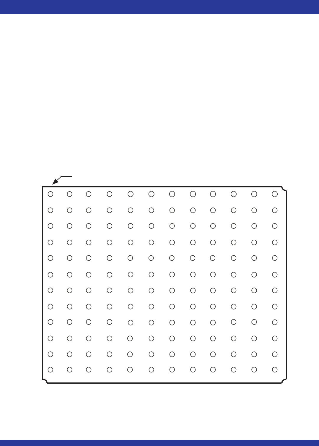
PIN CONFIGURATIONS (CONTINUED)
PBGA: 1mm pitch, 13mm x 13mm (BB144, order code: BB)
TOP VIEW
ASYW WEN
WCLK
PAF
FF/IR
HF BM EF
RCLK
REN OE
Q35
SEN
IW
PRS LD MRS
FS0 FS1
ASYR
IP PFM
RT
Q34
D35
D34
D33 FWFT/SI OW V
CC VCC
BE PAE
RM Q32 Q3
3
D32 D31 D30 V
CC VCC GND GND VCC VCC Q29 Q30 Q31
D29
D26
D27 V
CC Q26 Q27
Q28
D28
D25 D24
Q23
Q24 Q25
D21 D22 D23 Q22 Q21 Q20
D18 D19 D20 V
CC Q19 Q18 Q17
D15 D16 D17 V
CC Q16 Q15 Q14
D12 D13 D14 D3 D0 V
CC VCC TDO Q2
Q13 Q12
Q11
D10 D6 D4
D1
TMS
TCK
Q0 Q3 Q5 Q10 Q9
D8
D7 D5
D2
TRST
TDI Q1 Q4 Q6 Q7 Q8
A1 BALL PAD CORNER
A
B
C
D
E
F
G
H
J
K
L
M
12 3 4 5 6 7 8 9 1011 12
4667 drw02b
GND GND GND GND
GND GND GND GND
VCC
GND GND GND GND
VCC
GND
GND V
CC VCC
GND GND GND GND
D11
D9
V
CC
VCC
VCC
VCC
VCC
WCLK when WEN is asserted. During Asynchronous operation only the WR
input is used to write data into the FIFO. Data is written on a rising edge of WR,
the WEN input should be tied to its active state, (LOW).
The output port can be selected as either a Synchronous (clocked) interface,
or Asynchronous interface. During Synchronous operation the output port is
controlled by a Read Clock (RCLK) input and Read Enable (REN) input. Data
is read from the FIFO on every rising edge of RCLK when REN is asserted.
During Asynchronous operation only the RD input is used to read data from the
FIFO. Data is read on a rising edge of RD, the REN input should be tied to its
active state, LOW. When Asynchronous operation is selected on the output port
the FIFO must be configured for Standard IDT mode, and the OE input used
to provide three-state control of the outputs, Qn.
The frequencies of both the RCLK and the WCLK signals may vary from 0
to fMAX with complete independence. There are no restrictions on the frequency
of the one clock input with respect to the other.
There are two possible timing modes of operation with these devices: IDT
Standard mode and First Word Fall Through (FWFT) mode.
In IDT Standard mode, the first word written to an empty FIFO will not appear
on the data output lines unless a specific read operation is performed. A read
operation, which consists of activating REN and enabling a rising RCLK edge,
will shift the word from internal memory to the data output lines.
In FWFT mode, the first word written to an empty FIFO is clocked directly
to the data output lines after three transitions of the RCLK signal. A REN does
not have to be asserted for accessing the first word. However, subsequent

72V3640L6BB

Mfr. #:
Manufacturer:
IDT
Description:
FIFO 3.3V 32K X 36 SSII
Lifecycle:
New from this manufacturer.
Delivery:
DHL FedEx Ups TNT EMS
Payment:
T/T Paypal Visa MoneyGram Western Union