22
COMMERCIAL AND INDUSTRIAL
TEMPERATURE RANGES
IDT72V3640/50/60/70/80/90 3.3V HIGH DENSITY SUPERSYNC II
TM
36-BIT FIFO
1,024 x 36, 2,048 x 36, 4,096 x 36, 8,192 x 36, 16,384 x 36 and 32,768 x 36
If asynchronous PAE configuration is selected, the PAE is asserted LOW
on the LOW-to-HIGH transition of the Read Clock (RCLK). PAE is reset to HIGH
on the LOW-to-HIGH transition of the Write Clock (WCLK). If synchronous PAE
configuration is selected, the PAE is updated on the rising edge of RCLK. See
Figure 21, Asynchronous Programmable Almost-Empty Flag Timing (IDT
Standard and FWFT Mode).
HALF-FULL FLAG ( HF )
This output indicates a half-full FIFO. The rising WCLK edge that fills the FIFO
beyond half-full sets HF LOW. The flag remains LOW until the difference between
the write and read pointers becomes less than or equal to half of the total depth
of the device; the rising RCLK edge that accomplishes this condition sets HF
HIGH.
In IDT Standard mode, if no reads are performed after reset (MRS or PRS),
HF will go LOW after (D/2 + 1) writes to the FIFO, where D = 1,024 for the
IDT72V3640, 2,048 for the IDT72V3650, 4,096 for the IDT72V3660, 8,192
for the IDT72V3670, 16,384 for the IDT72V3680 and 32,768 for the IDT72V3690.
In FWFT mode, if no reads are performed after reset (MRS or PRS), HF
will go LOW after (D-1/2 + 2) writes to the FIFO, where D = 1,025 for the
IDT72V3640, 2,049 for the IDT72V3650, 4,097 for the IDT72V3660, 8,193 for
the IDT72V3670, 16,385 for the IDT72V3680 and 32,769 for the IDT72V3690.
See Figure 22, Half-Full Flag Timing (IDT Standard and FWFT Modes),
for the relevant timing information. Because HF is updated by both RCLK and
WCLK, it is considered asynchronous.
DATA OUTPUTS (Q0-Qn)
(Q0-Q35) are data outputs for 36-bit wide data, (Q0 - Q17) are data outputs
for 18-bit wide data or (Q0-Q8) are data outputs for 9-bit wide data.
23
COMMERCIAL AND INDUSTRIAL
TEMPERATURE RANGES
IDT72V3640/50/60/70/80/90 3.3V HIGH DENSITY SUPERSYNC II
TM
36-BIT FIFO
1,024 x 36, 2,048 x 36, 4,096 x 36, 8,192 x 36, 16,384 x 36 and 32,768 x 36
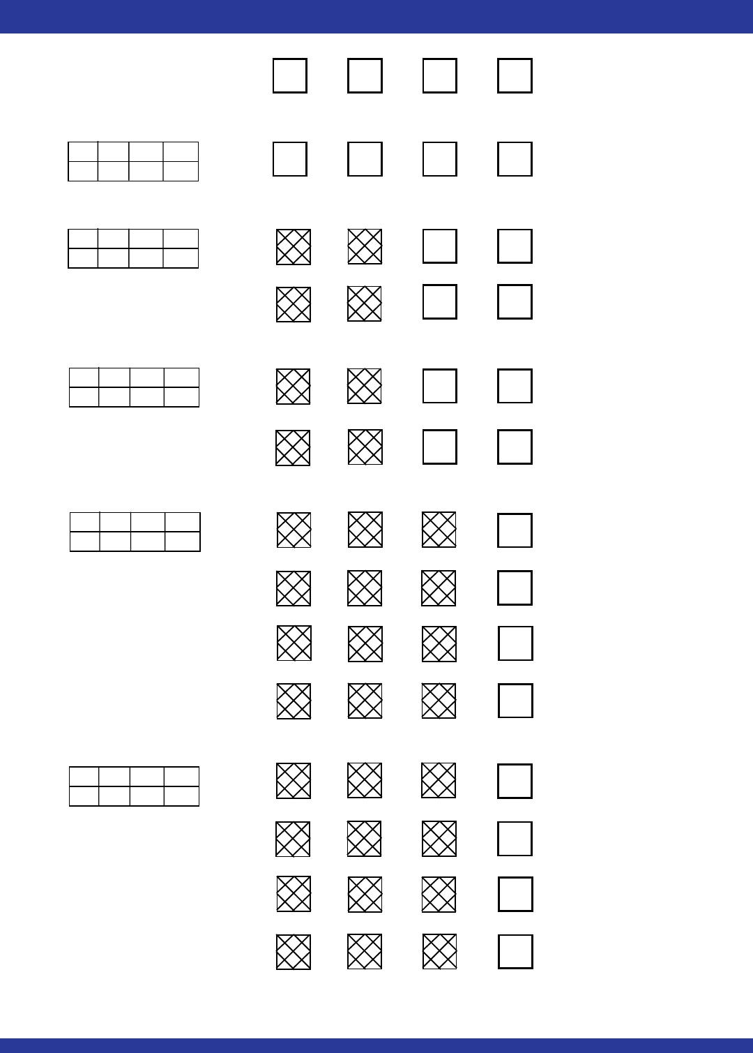
D35-D27 D26-D18 D17-D9 D8-D0
A
A
A
D
A
C
B
B
B
C
B
D
C
C
C
A
D
D
D
B
(a) x36 INPUT to x36 OUTPUT
(b) x36 INPUT to x18 OUTPUT - BIG-ENDIAN
(c) x36 INPUT to x18 OUTPUT - LITTLE-ENDIAN
(d) x36 INPUT to x9 OUTPUT - BIG-ENDIAN
Write to FIFO
Read from FIFO
1st: Read from FIFO
BE BM IW OW
BYTE ORDER ON INPUT PORT:
2nd: Read from FIFO
3rd: Read from FIFO
4th: Read from FIFO
1st: Read from FIFO
1st: Read from FIFO
2nd: Read from FIFO
2nd: Read from FIFO
D
C
(e) x36 INPUT to x9 OUTPUT - LITTLE-ENDIAN
1st: Read from FIFO
A
B
2nd: Read from FIFO
3rd: Read from FIFO
4th: Read from FIFO
4667 drw08
BYTE ORDER ON OUTPUT PORT:
L H L L
H H L L
L H L H
H H L H
X L L L
BE BM IW OW
BE BM IW OW
BE BM IW OW
BE BM IW OW
Q35-Q27 Q26-Q18 Q17-Q9 Q8-Q0
Figure 4. Bus-Matching Byte Arrangement
24
COMMERCIAL AND INDUSTRIAL
TEMPERATURE RANGES
IDT72V3640/50/60/70/80/90 3.3V HIGH DENSITY SUPERSYNC II
TM
36-BIT FIFO
1,024 x 36, 2,048 x 36, 4,096 x 36, 8,192 x 36, 16,384 x 36 and 32,768 x 36
Q35-Q27 Q26-Q18 Q17-Q9 Q8-Q0
A
A
D
A
C
B
B
C
B
D
C
D
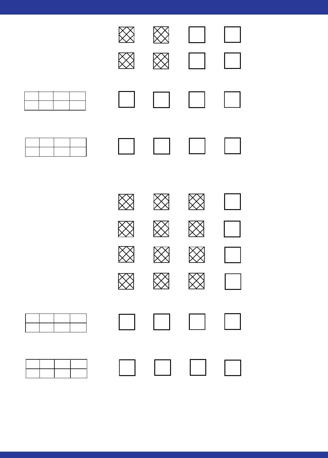
D35-D27 D26-D18 D17-D9 D8-D0
(a) x18 INPUT to x36 OUTPUT - BIG-ENDIAN
Read from FIFO
1st: Write to FIFO
BYTE ORDER ON INPUT PORT:
2nd: Write to FIFO
3rd: Write to FIFO
4th: Write to FIFO
D35-D27 D26-D18 D17-D9 D8-D0
1st: Write to FIFO
2nd: Write to FIFO
4667 drw09
BYTE ORDER ON OUTPUT PORT:
Q35-Q27 Q26-Q18 Q17-Q9 Q8-Q0
C
D
A
B
(b) x18 INPUT to x36 OUTPUT - LITTLE-ENDIAN
Read from FIFO
BE BM IW OW
H H H L
BYTE ORDER ON INPUT PORT:
ABCD
(a) x9 INPUT to x36 OUTPUT - BIG-ENDIAN
Read from FIFO
BE BM IW OW
L H H H
BYTE ORDER ON OUTPUT PORT:
D
C
B
A
(b) x9 INPUT to x36 OUTPUT - LITTLE-ENDIAN
Read from FIFO
BE BM IW OW
H H H H
BE BM IW OW
L H H L
D35-D27 D26-D18 D17-D9 D8-D0
Q35-Q27 Q26-Q18 Q17-Q9 Q8-Q0
Figure 4. Bus-Matching Byte Arrangement (Continued)

72V3640L6BB

Mfr. #:
Manufacturer:
IDT
Description:
FIFO 3.3V 32K X 36 SSII
Lifecycle:
New from this manufacturer.
Delivery:
DHL FedEx Ups TNT EMS
Payment:
T/T Paypal Visa MoneyGram Western Union