27
COMMERCIAL AND INDUSTRIAL
TEMPERATURE RANGES
IDT72V3640/50/60/70/80/90 3.3V HIGH DENSITY SUPERSYNC II
TM
36-BIT FIFO
1,024 x 36, 2,048 x 36, 4,096 x 36, 8,192 x 36, 16,384 x 36 and 32,768 x 36
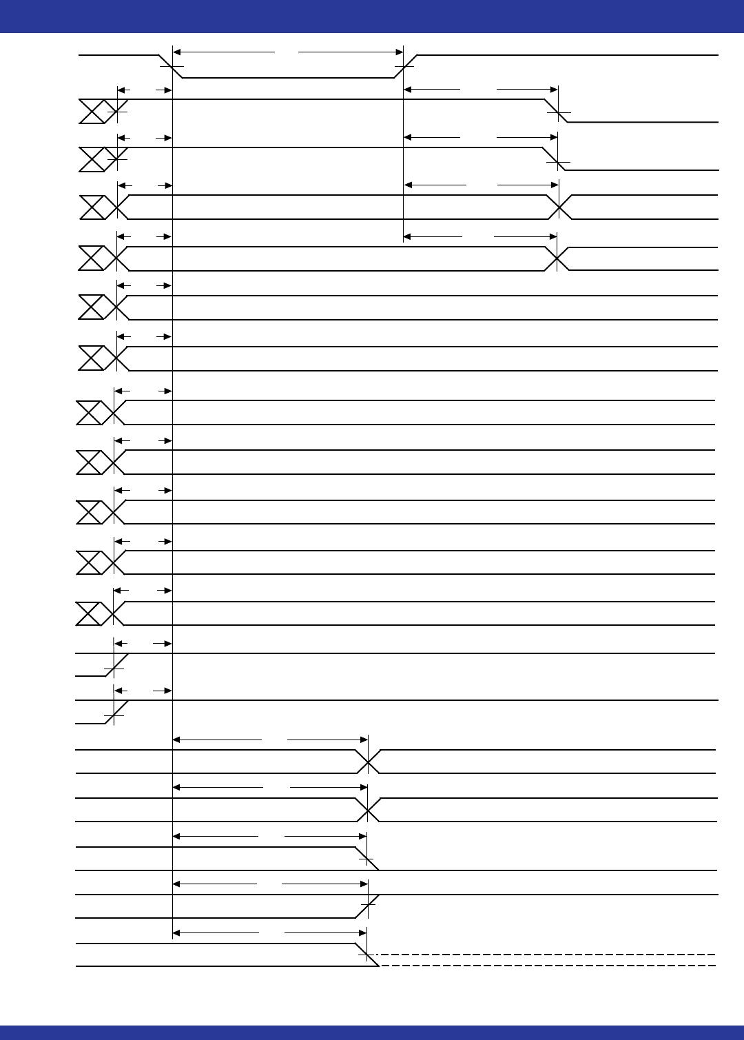
Figure 8. Read Cycle, Empty Flag and First Data Word Latency Timing (IDT Standard Mode)
NOTES:
1. tSKEW1 is the minimum time between a rising WCLK edge and a rising RCLK edge to guarantee that EF will go HIGH (after one RCLK cycle plus tREF). If the time between the rising edge
of WCLK and the rising edge of RCLK is less than tSKEW1, then EF deassertion may be delayed one extra RCLK cycle.
2. LD = HIGH.
3. First data word latency = tSKEW1 + 1*TRCLK + tREF.
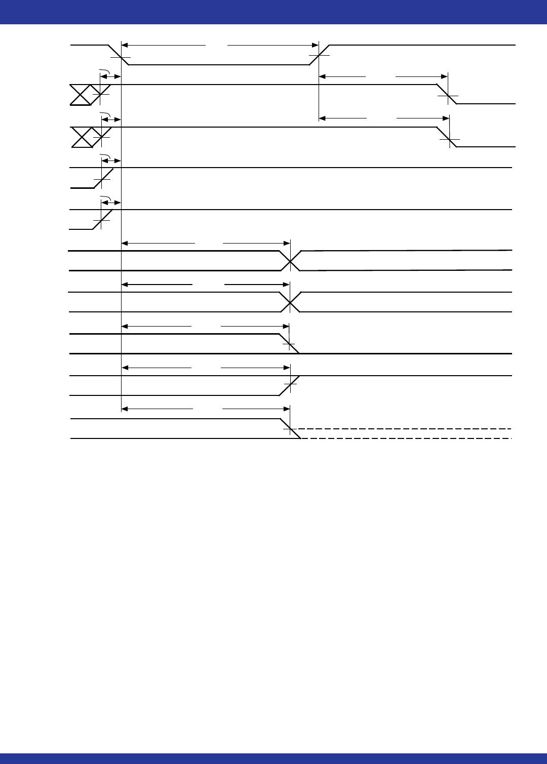
NOTES:
1. t
SKEW1 is the minimum time between a rising RCLK edge and a rising WCLK edge to guarantee that FF will go HIGH (after one WCLK cycle pus tWFF). If the time between
the rising edge of the RCLK and the rising edge of the WCLK is less than tSKEW1, then the FF deassertion may be delayed one extra WCLK cycle.
2. LD = HIGH, OE = LOW, EF = HIGH
Figure 7. Write Cycle and Full Flag Timing (IDT Standard Mode)
NO OPERATION
RCLK
REN
4667 drw13
EF
t
CLK
t
CLKH
t
CLKL
t
ENH
t
REF
t
A
t
OLZ
t
OE
Q0 - Qn
OE
WCLK
(1)
t
SKEW1
WEN
D0 - Dn
t
ENS
t
ENS
t
ENH
t
DS
t
DH
D
0
1
2
t
OLZ
NO OPERATION
LAST WORD
D
0
D
1
D
1
t
ENS
t
ENH
t
DS
t
DH
t
OHZ
LAST WORD
t
REF
t
ENH
t
ENS
t
A
t
A
t
REF
t
ENS
t
ENH
D
0
- D
n
WEN
RCLK
REN
t
ENH
t
ENH
Q
0
- Q
n
DATA READ
NEXT DATA READDATA IN OUTPUT REGISTER
t
SKEW1
(1)
4667 drw12
WCLK
NO WRITE
1
2
1
2
t
DS
NO WRITE
t
WFF
t
WFF
t
WFF
t
A
t
ENS
t
ENS
t
SKEW1
(1)
t
DS
t
A
D
X
t
DH
t
CLK
t
CLKH
t
CLKL
D
X
+1
t
WFF
t
DH
FF