4
COMMERCIAL AND INDUSTRIAL
TEMPERATURE RANGES
IDT72V3640/50/60/70/80/90 3.3V HIGH DENSITY SUPERSYNC II
TM
36-BIT FIFO
1,024 x 36, 2,048 x 36, 4,096 x 36, 8,192 x 36, 16,384 x 36 and 32,768 x 36
Figure 1. Single Device Configuration Signal Flow Diagram
words written to the FIFO do require a LOW on REN for access. The state of
the FWFT/SI input during Master Reset determines the timing mode in use.
For applications requiring more data storage capacity than a single FIFO
can provide, the FWFT timing mode permits depth expansion by chaining FIFOs
in series (i.e. the data outputs of one FIFO are connected to the corresponding
data inputs of the next). No external logic is required.
These FIFOs have five flag pins, EF/OR (Empty Flag or Output Ready),
FF/IR (Full Flag or Input Ready), HF (Half-full Flag), PAE (Programmable
Almost-Empty flag) and PAF (Programmable Almost-Full flag). The EF and FF
functions are selected in IDT Standard mode. The IR and OR functions are
selected in FWFT mode. HF, PAE and PAF are always available for use,
irrespective of timing mode.
PAE and PAF can be programmed independently to switch at any point in
memory. Programmable offsets determine the flag switching threshold and can
be loaded by two methods: parallel or serial. Eight default offset settings are also
provided, so that PAE can be set to switch at a predefined number of locations
from the empty boundary and the PAF threshold can also be set at similar
predefined values from the full boundary. The default offset values are set during
Master Reset by the state of the FSEL0, FSEL1, and LD pins.
For serial programming, SEN together with LD on each rising edge of
WCLK, are used to load the offset registers via the Serial Input (SI). For parallel
programming, WEN together with LD on each rising edge of WCLK, are used
to load the offset registers via D
n. REN together with LD on each rising edge
of RCLK can be used to read the offsets in parallel from Qn regardless of whether
serial or parallel offset loading has been selected.
During Master Reset (MRS) the following events occur: the read and write
pointers are set to the first location of the FIFO. The FWFT pin selects IDT
Standard mode or FWFT mode.
The Partial Reset (PRS) also sets the read and write pointers to the first
location of the memory. However, the timing mode, programmable flag
programming method, and default or programmed offset settings existing before
Partial Reset remain unchanged. The flags are updated according to the timing
mode and offsets in effect. PRS is useful for resetting a device in mid-operation,
when reprogramming programmable flags would be undesirable.
It is also possible to select the timing mode of the PAE (Programmable Almost-
Empty flag) and PAF (Programmable Almost-Full flag) outputs. The timing
modes can be set to be either asynchronous or synchronous for the PAE and
PAF flags.
(x36, x18, x9) DATA OUT (Q0 - Qn)(x36, x18, x9) DATA IN (D0 - Dn)
MASTER RESET (MRS)
READ CLOCK (RCLK/RD*)
READ ENABLE (REN)
OUTPUT ENABLE (OE)
EMPTY FLAG/OUTPUT READY (EF/OR)
PROGRAMMABLE ALMOST-EMPTY (PAE)
WRITE CLOCK (WCLK/WR*)
WRITE ENABLE (WEN)
LOAD (LD)
FULL FLAG/INPUT READY (FF/IR)
PROGRAMMABLE ALMOST-FULL (PAF)
IDT
72V3640
72V3650
72V3660
72V3670
72V3680
72V3690
PARTIAL RESET (PRS)
FIRST WORD FALL THROUGH/
SERIAL INPUT (FWFT/SI)
RETRANSMIT (RT)
4667 drw03
HALF-FULL FLAG (HF)
SERIAL ENABLE(SEN)
INPUT WIDTH (IW)
OUTPUT WIDTH (OW)
BIG-ENDIAN/LITTLE-ENDIAN (BE)
INTERSPERSED/
NON-INTERSPERSED PARITY (IP)
BUS-
MATCHING
(BM)
5
COMMERCIAL AND INDUSTRIAL
TEMPERATURE RANGES
IDT72V3640/50/60/70/80/90 3.3V HIGH DENSITY SUPERSYNC II
TM
36-BIT FIFO
1,024 x 36, 2,048 x 36, 4,096 x 36, 8,192 x 36, 16,384 x 36 and 32,768 x 36
BM IW OW Write Port Width Read Port Width
L L L x36 x36
H L L x36 x18
H L H x36 x9
H H L x18 x36
H H H x9 x36
TABLE 1 — BUS-MATCHING CONFIGURATION MODES
If asynchronous PAE/PAF configuration is selected, the PAE is asserted
LOW on the LOW-to-HIGH transition of RCLK. PAE is reset to HIGH on the LOW-
to-HIGH transition of WCLK. Similarly, the PAF is asserted LOW on the LOW-
to-HIGH transition of WCLK and PAF is reset to HIGH on the LOW-to-HIGH
transition of RCLK.
If synchronous PAE/PAF configuration is selected , the PAE is asserted and
updated on the rising edge of RCLK only and not WCLK. Similarly, PAF is
asserted and updated on the rising edge of WCLK only and not RCLK. The mode
desired is configured during MasterReset by the state of the Programmable Flag
Mode (PFM) pin.
The Retransmit function allows data to be reread from the FIFO more than
once. A LOW on the RT input during a rising RCLK edge initiates a retransmit
operation by setting the read pointer to the first location of the memory array.
A zero-latency retransmit timing mode can be selected using the Retransmit
timing Mode pin (RM). During Master Reset, a LOW on RM will select zero
latency retransmit. A HIGH on RM during Master Reset will select normal
latency.
If zero latency retransmit operation is selected, the first data word to be
retransmitted will be placed on the output register with respect to the same RCLK
edge that initiated the retransmit based on RT being LOW.
Refer to Figure 11 and 12 for Retransmit Timing with normal latency. Refer
to Figure 13 and 14 for Zero Latency Retransmit Timing.
The device can be configured with different input and output bus widths as
shown in Table 1.
A Big-Endian/Little-Endian data word format is provided. This function is
useful when data is written into the FIFO in long word format (x36/x18) and read
NOTE:
1. Pin status during Master Reset.
out of the FIFO in small word (x18/x9) format. If Big-Endian mode is selected,
then the most significant byte (word) of the long word written into the FIFO will
be read out of the FIFO first, followed by the least significant byte. If Little-Endian
format is selected, then the least significant byte of the long word written into the
FIFO will be read out first, followed by the most significant byte. The mode desired
is configured during master reset by the state of the Big-Endian (BE) pin. See
Figure 4 for Bus-Matching Byte Arrangement.
The Interspersed/Non-Interspersed Parity (IP) bit function allows the user
to select the parity bit in the word loaded into the parallel port (D
0-Dn) when
programming the flag offsets. If Interspersed Parity mode is selected, then the
FIFO will assume that the parity bit is located in bit positions D8, D17, D26 and
D35 during the parallel programming of the flag offsets. If Non-Interspersed
Parity mode is selected, then D8, D17 and D26 are assumed to be valid bits
and D32, D33, D34 and D35 are ignored. IP mode is selected during Master
Reset by the state of the IP input pin. Interspersed Parity control only has an
effect during parallel programming of the offset registers. It does not effect the data
written to and read from the FIFO.
A JTAG test port is provided, here the FIFO has fully functional Boundary
Scan feature, compliant with IEEE 1149.1 Standard Test Access Port and
Boundary Scan Architecture.
If, at any time, the FIFO is not actively performing an operation, the chip will
automatically power down. Once in the power down state, the standby supply
current consumption is minimized. Initiating any operation (by activating control
inputs) will immediately take the device out of the power down state.
The IDT72V3640/72V3650/72V3660/72V3670/72V3680/72V3690 are
fabricated using IDT’s high speed submicron CMOS technology.
6
COMMERCIAL AND INDUSTRIAL
TEMPERATURE RANGES
IDT72V3640/50/60/70/80/90 3.3V HIGH DENSITY SUPERSYNC II
TM
36-BIT FIFO
1,024 x 36, 2,048 x 36, 4,096 x 36, 8,192 x 36, 16,384 x 36 and 32,768 x 36
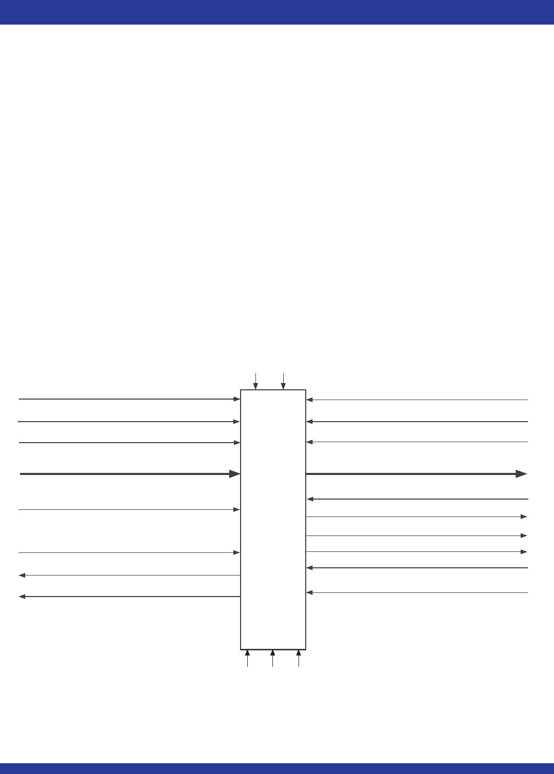
PIN DESCRIPTION (TQFP AND PBGA PACKAGES)
Symbol Name I/O Description
BM
(1)
Bus-Matching I BM works with IW and OW to select the bus sizes for both write and read ports. See Table 1 for bus size configuration.
BE
(1)
Big-Endian/ I During Master Reset, a LOW on BE will select Big-Endian operation. A HIGH on BE during Master Reset will
Little-Endian select Little-Endian format.
D0–D35 Data Inputs I Data inputs for a 36-, 18- or 9-bit bus. When in 18- or 9-bit mode, the unused input pins are in a don’t care state.
EF/OR Empty Flag/ O In the IDT Standard mode, the EF function is selected. EF indicates whether or not the FIFO memory is empty.
Output Ready In FWFT mode, the OR function is selected. OR indicates whether or not there is valid data available at the outputs.
FF/IR Full Flag/ O In the IDT Standard mode, the FF function is selected. FF indicates whether or not the FIFO memory is full. In the
Input Ready FWFT mode, the IR function is selected. IR indicates whether or not there is space available for writing to the FIFO
memory.
FSEL0
(1)
Flag Select Bit 0 I During Master Reset, this input along with FSEL1 and the LD pin, will select the default offset values for the programmable
flags PAE and PAF. There are up to eight possible settings available.
FSEL1
(1)
Flag Select Bit 1 I During Master Reset, this input along with FSEL0 and the LD pin will select the default offset values for the programmable
flags PAE and PAF. There are up to eight possible settings available.
FWFT/SI First Word Fall I During Master Reset, selects First Word Fall Through or IDT Standard mode. After Master Reset, this pin functions
Through/Serial In as a serial input for loading offset registers.
HF Half-Full Flag O HF indicates whether the FIFO memory is more or less than half-full.
IP
(1)
Interspersed Parity I During Master Reset, a LOW on IP will select Non-Interspersed Parity mode. A HIGH will select Interspersed Parity
mode. Interspersed Parity control only has an effect during parallel programming of the offset registers. It does not
effect the data written to and read from the FIFO.
IW
(1)
Input Width I This pin, along with OW and MB, selects the bus width of the write port. See Table 1 for bus size configuration.
LD Load I This is a dual purpose pin. During Master Reset, the state of the LD input along with FSEL0 and FSEL1, determines
one of eight default offset values for the PAE and PAF flags, along with the method by which these offset registers can
be programmed, parallel or serial (see Table 2). After Master Reset, this pin enables writing to and reading from the
offset registers.
OE Output Enable I OE controls the output impedance of Qn.
OW
(1)
Output Width I This pin, along with IW and BM, selects the bus width of the read port. See Table 1 for bus size configuration.
MRS Master Reset I MRS initializes the read and write pointers to zero and sets the output register to all zeroes. During Master Reset,
the FIFO is configured for either FWFT or IDT Standard mode, Bus-Matching configurations, one of eight progammable
flag default settings, serial or parallel programming of the offset settings, Big-Endian/Little-Endian format, zero latency
timing mode, interspersed parity, and synchronous versus asynchronous programmable flag timing modes.
PAE Programmable O PAE goes LOW if the number of words in the FIFO memory is less than offset n, which is stored in the Empty Offset
Almost-Empty Flag register. PAE goes HIGH if the number of words in the FIFO memory is greater than or equal to offset n.
PAF Programmable O PAF goes HIGH if the number of free locations in the FIFO memory is more than offset m, which is stored in the
Almost-Full Flag Full Offset register. PAF goes LOW if the number of free locations in the FIFO memory is less than or equal to m.
PFM
(1)
Programmable I During Master Reset, a LOW on PFM will select Asynchronous Programmable flag timing mode. A HIGH on PFM
Flag Mode will select Synchronous Programmable flag timing mode.
PRS Partial Reset I PRS initializes the read and write pointers to zero and sets the output register to all zeroes. During Partial Reset,
the existing mode (IDT or FWFT), programming method (serial or parallel), and programmable flag settings are all
retained.
Q0–Q35 Data Outputs O Data outputs for an 36-, 18- or 9-bit bus. When in 18- or 9-bit mode, the unused output pins are in a don’t care
state. Outputs are not 5V tolerant regardless of the state of OE.
RCLK/ Read Clock/ I If Synchronous operation of the read port has been selected, when enabled by REN, the rising edge of RCLK
RD Read Strobe reads data from the FIFO memory and offsets from the programmable registers. If LD is LOW, the values loaded
into the offset registers is output on a rising edge of RCLK.If Asynchronous operation of the read port has been
selected, a rising edge on RD reads data from the FIFO in an Asynchronous manner. REN should be tied LOW.
Asynchronous operation of the RCLK/RD input is only available in the PBGA package.
REN Read Enable I REN enables RCLK for reading data from the FIFO memory and offset registers.
RM
(1)
Retransmit Timing I During Master Reset, a LOW on RM will select zero latency Retransmit timing Mode. A HIGH on RM will select
Mode normal latency mode.
RT Retransmit I RT asserted on the rising edge of RCLK initializes the READ pointer to zero, sets the EF flag to LOW (OR to HIGH
in FWFT mode) and does not disturb the write pointer, programming method, existing timing mode or programmable
flag settings. RT is useful to reread data from the first physical location of the FIFO.
NOTE:
1. Inputs should not change state after Master Reset.

72V3640L6BB

Mfr. #:
Manufacturer:
IDT
Description:
FIFO 3.3V 32K X 36 SSII
Lifecycle:
New from this manufacturer.
Delivery:
DHL FedEx Ups TNT EMS
Payment:
T/T Paypal Visa MoneyGram Western Union