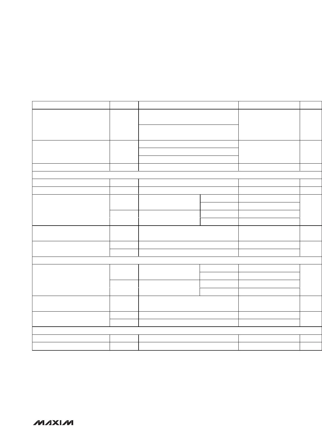
General Description
The MAX15018A/MAX15018B/MAX15019A/MAX15019B
high-frequency, 125V half-bridge, n-channel MOSFET
drivers drive high- and low-side MOSFETs in high-volt-
age applications. These drivers are independently con-
trolled, and their 35ns (typ) propagation delay, from input
to output, are matched to within 2ns (typ). The high-volt-
age operation with very low and matched propagation
delay between drivers, and high source-/sink-current
capabilities in a thermally enhanced package make
these devices suitable for high-power, high-frequency
telecom power converters. The 125V maximum input
voltage provides plenty of margin over the 100V input
transient requirement of telecom standards. A reliable
on-chip bootstrap diode connected between V
DD
and
BST eliminates the need for an external discrete diode.
The MAX15018A/MAX15019A both offer noninverting dri-
vers. The MAX15018B/MAX15019B offer a noninverting
high-side driver and an inverting low-side driver (see the
Selector Guide
.) The MAX15018_ feature CMOS (V
DD
/2)
logic inputs. The MAX15019_ feature TTL-logic inputs.
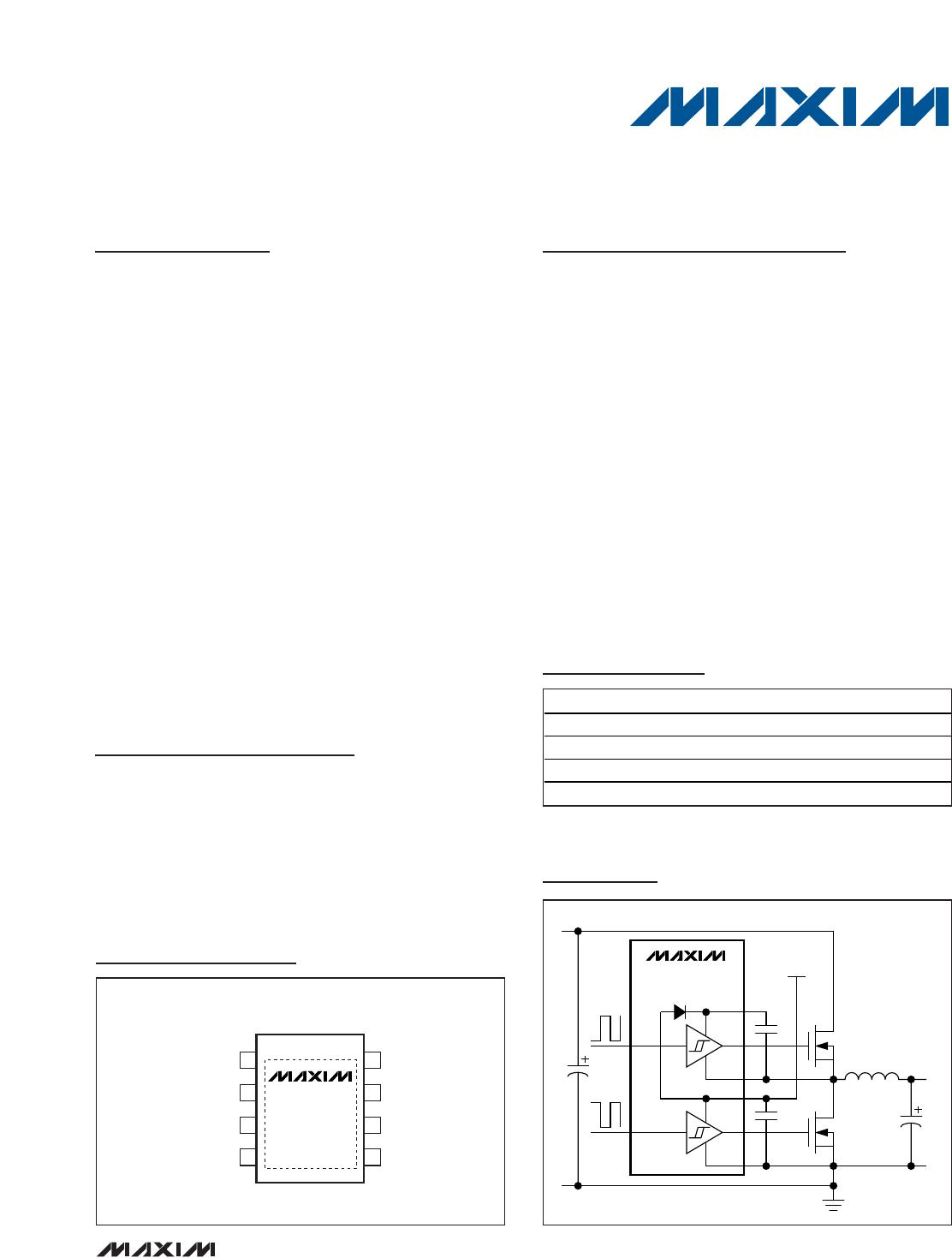
The drivers are available in the industry-standard 8-pin
SO footprint and pin configuration with a thermally
enhanced 8-pin SO package. All devices operate over
the -40°C to +125°C automotive temperature range.
Applications
Telecom Power Supplies
Synchronous Buck DC-to-DC Converters
Half-Bridge, Full-Bridge, and Two-Switch
Forward Converters
Power-Supply Modules
Motor Control
Features
o HIP2100IB/HIP2101IB Pin Compatible
(MAX15018A/MAX15019A)
o Up to 125V V
IN
Operation
o 8V to 12.6V V
DD
Input Supply Range
o 3A Peak Source and Sink Current
o 35ns Propagation Delay
o Guaranteed 8ns or Less Propagation Delay
Matching Between High- and Low-Side Drivers
o Both Noninverting/Noninverting and
Noninverting/Inverting Logic-Input Versions
Available
o Up to 15V Logic Inputs, Independent of V
DD
Supply Voltage
o Low 8pF Input Capacitance
o Available in CMOS (V
DD
/2) or TTL Logic-Level
Inputs with Hysteresis
o Available in a Space-Saving, Thermally Enhanced
8-Pin SO-EP Package
MAX15018/MAX15019
125V/3A, High-Speed,
Half-Bridge MOSFET Drivers
________________________________________________________________
Maxim Integrated Products
1
MAX15018A
MAX15018B
MAX15019A
MAX15019B
81V
DD
DL
72BST GND
63DH IN_L
54HS IN_H
SO-EP
TOP VIEW
+
Pin Configuration
Ordering Information
MAX15018A
MAX15019A
BST
DH
HS
V
DD
DL
PWM1
PWM2
IN_H
IN_L
V
OUT
V
IN
= 0 TO 125V
N
N
C
BST
V
DD
= 8V TO
12.6V
C
VDD
GND
PART TEMP RANGE PIN-PACKAGE
MAX15018AASA+
-40°C to +125°C 8 SO-EP*
MAX15018BASA+
-40°C to +125°C 8 SO-EP*
MAX15019AASA+
-40°C to +125°C 8 SO-EP*
MAX15019BASA+
-40°C to +125°C 8 SO-EP*
Typical Operating Circuit
19-4146; Rev 1; 9/08
For pricing, delivery, and ordering information, please contact Maxim Direct at 1-888-629-4642,
or visit Maxim’s website at www.maxim-ic.com.
+
Denotes a lead-free/RoHS-compliant package.
*
EP = Exposed pad. Internally connected to GND.
MAX15018/MAX15019
125V/3A, High-Speed,
Half-Bridge MOSFET Drivers
2 _______________________________________________________________________________________
ABSOLUTE MAXIMUM RATINGS
ELECTRICAL CHARACTERISTICS
(V
DD
= V
BST
= 8V to 12.6V, V
HS
= V
GND
= 0V, T
A
= T
J
= -40°C to +125°C, unless otherwise noted. Typical values are at V
DD
= V
BST
= 12V and T
A
= +25°C.) (Note 1)
Stresses beyond those listed under “Absolute Maximum Ratings” may cause permanent damage to the device. These are stress ratings only, and functional
operation of the device at these or any other conditions beyond those indicated in the operational sections of the specifications is not implied. Exposure to
absolute maximum rating conditions for extended periods may affect device reliability.
V
DD
to GND............................................................-0.3V to +15V
IN_H, IN_L to GND .................................................-0.3V to +15V
DL to GND..................................................-0.3V to (V
DD
+ 0.3V)
DH to HS.....................................................-0.3V to (V
DD
+ 0.3V)
BST to HS ...............................................................-0.3V to +15V
HS to GND (repetitive transient)..............................-5V to +130V
HS dv/dt to GND................................................................50V/ns
Continuous Power Dissipation (T
A
= +70°C)
Single and Multilayer Board
8-Pin SO-EP (derate 23.8mW/°C above +70°C)*..........1.904W
θ
JC
...................................................................................6°C/W
Operating Temperature .....................................-40°C to +125°C
Maximum Junction Temperature .....................................+150°C
Storage Temperature Range .............................-65°C to +150°C
Lead Temperature (soldering, 10s) .................................+300°C
PARAMETER SYMBOL CONDITIONS MIN TYP MAX UNITS
POWER SUPPLY
Operating Supply Voltage V
VDD
8.0 12.6 V
MAX15018A/
MAX15018B
65 130
V
DD
Quiescent Supply Current I
DDQ
IN_H and IN_L are
unconnected (no
switching)
MAX15019A/
MAX15019B
95 190
µA
V
DD
Operating Supply Current I
DDO
f
SW
= 500kHz, V
DD
= 12V,
no capacitive load
2.75 3.75 mA
BST Quiescent Supply Current I
BSTQ
IN_H and IN_L are unconnected (no
switching)
95 190 µA
BST Operating Supply Current I
BSTO
f
SW
= 500kHz, V
BST
- V
HS
= 12V, no
capacitive load
2.75 3.75 mA
UVLO (V
DD
to GND) V
DD_UVLO
V
DD
rising 6.5 7.3 8 V
UVLO (BST to HS) V
BST_UVLO
V
BST
rising 6.2 6.9 7.6 V
UVLO Hysteresis 0.5 V
LOGIC INPUT
MAX15018A/MAX15018B (CMOS)
0.67 x
V
DDInput-Logic High V
IH
MAX15019A/MAX15019B (TTL) 2
V
MAX15018A/MAX15018B (CMOS)
0.33 x
V
DD
Input-Logic Low V
IL
MAX15019A/MAX15019B (TTL) 0.8
V
MAX15018A/MAX15018B (CMOS) 1.65
Logic-Input Hysteresis V
HYS
MAX15019A/MAX15019B (TTL) 0.4
V
*
As per JEDEC Standard 51 (Single-Layer Board).
MAX15018/MAX15019
125V/3A, High-Speed,
Half-Bridge MOSFET Drivers
_______________________________________________________________________________________ 3
PARAMETER SYMBOL CONDITIONS MIN TYP MAX UNITS
IN_H = IN_L = GND
(MAX15018A/MAX15019A)
Logic-Input Current I
IN_
IN_H = GND, IN_L = V
DD
(MAX15018B/MAX15019B)
-1 +1 µA
IN_L to GND (MAX15018A/MAX15019A)
IN_L to V
DD
(MAX15018B/MAX15019B)
Input Resistance R
IN_
IN_H to GND
5001 k
Input Capacitance C
IN_
8pF
HIGH-SIDE GATE DRIVER
HS Maximum Voltage V
HS_MAX
125 V
BST Maximum Voltage V
BST_MAX
140 V
T
A
= +25°C 1.75 2.4
R
ON_HP
(V
BST
- V
HS
) = 12V,
I
DH
= 100mA (sourcing)
T
A
= +125°C 2.3 3.0
T
A
= +25°C 1.1 1.75
Driver Output Resistance
R
ON_HN
(V
BST
- V
HS
) = 12V, I
DH
=
100mA (sinking)
T
A
= +125°C 1.6 2.25
Power-Off Pulldown Clamp
Voltage
V
BST
= 0V or unconnected, I
DH
= 1mA
(sinking)
0.88 1.2 V
I
PK_HP
V
DH
= 0V 3
Peak Output Current
I
PK_HN
V
DH
= 12V 3
A
LOW-SIDE GATE DRIVER
T
A
= +25°C 1.75 2.4
R
ON_LP
V
DD
= 12V,
I
DL
= 100mA (sourcing)
T
A
= +125°C 2.3 3.0
T
A
= +25°C 1.1 1.75
Driver Output Resistance
R
ON_LN
V
DD
= 12V,
I
DL
= 100mA (sinking)
T
A
= +125°C 1.6 2.25
Power-Off Pulldown Clamp
Voltage
V
DD
= 0V or unconnected, I
DL
= 1mA
(sinking)
0.88 1.2 V
I
PK_LP
V
DL
= 0V 3
Peak Output Current
I
PK_LN
V
DL
= 12V 3
A
INTERNAL BOOTSTRAP DIODE
Forward Voltage Drop V
F
I
BST
= 100mA 0.9 1.1 V
Turn-On and Turn-Off Time t
RR
I
BST
= 100mA 40 ns
ELECTRICAL CHARACTERISTICS (continued)
(V
DD
= V
BST
= 8V to 12.6V, V
HS
= V
GND
= 0V, T
A
= T
J
= -40°C to +125°C, unless otherwise noted. Typical values are at V
DD
= V
BST
= 12V and T
A
= +25°C.) (Note 1)

MAX15019BASA+T

Mfr. #:
Manufacturer:
Maxim Integrated
Description:
Gate Drivers 125V/3A High-Speed Half-B MOSFET Drvr
Lifecycle:
New from this manufacturer.
Delivery:
DHL FedEx Ups TNT EMS
Payment:
T/T Paypal Visa MoneyGram Western Union