MAX15018/MAX15019
Bootstrap Capacitor
The bootstrap capacitor is used to ensure adequate
charge is available to switch the high-side MOSFET.
This capacitor is charged from V
DD
through the internal
bootstrap diode when the low-side MOSFET is on. The
bootstrap capacitor value should be selected carefully
to avoid oscillations during turn-on and turn-off at the
DH output. Choose a capacitor value approximately 20
times greater than the total gate capacitance of the
MOSFET being switched. Use a low-ESR, X7R-type
dielectric ceramic capacitor (typically a 0.1µF ceramic
is adequate). The high-side MOSFET’s continuous on-
time is limited due to the charge loss from the high-side
driver’s quiescent current. The maximum on-time is
dependent on the size of C
BST
, I
BST
(190µA max), and
V
BST_UVLO.
Note that the bootstrap capacitor requires
time to charge up to V
DD
, according to the time con-
stant of the charging loop through the lower MOSFET
(see the
Typical Operating Circuit
). Ensure that the
lower MOSFET is on for at least the minimum time
required to charge C
BST
.
Driver Logic Inputs (IN_H, IN_L)
The MAX15018_ are CMOS (V
DD
/2) logic-input drivers,
and the MAX15019_ are TTL-compatible logic-input dri-
vers. The required logic-input levels are independent of
V
DD
. For example, the IC can be powered by a 10V sup-
ply while the logic inputs are provided from 12V CMOS
logic. Additionally, the logic inputs are protected against
voltage spikes up to 15V, regardless of V
DD
voltage. The
TTL and CMOS logic inputs have 400mV and 1.6V hys-
teresis, respectively, to avoid double pulsing during sig-
nal transition. The logic inputs are high-impedance pins
(500kΩ typ) and should not be left unconnected to
ensure the input logic state is at a known level. With the
logic inputs unconnected, the DH and DL outputs pull
low as V
DD
rises up above the UVLO threshold. The
PWM output from the controller must assume a proper
state while powering up the device.
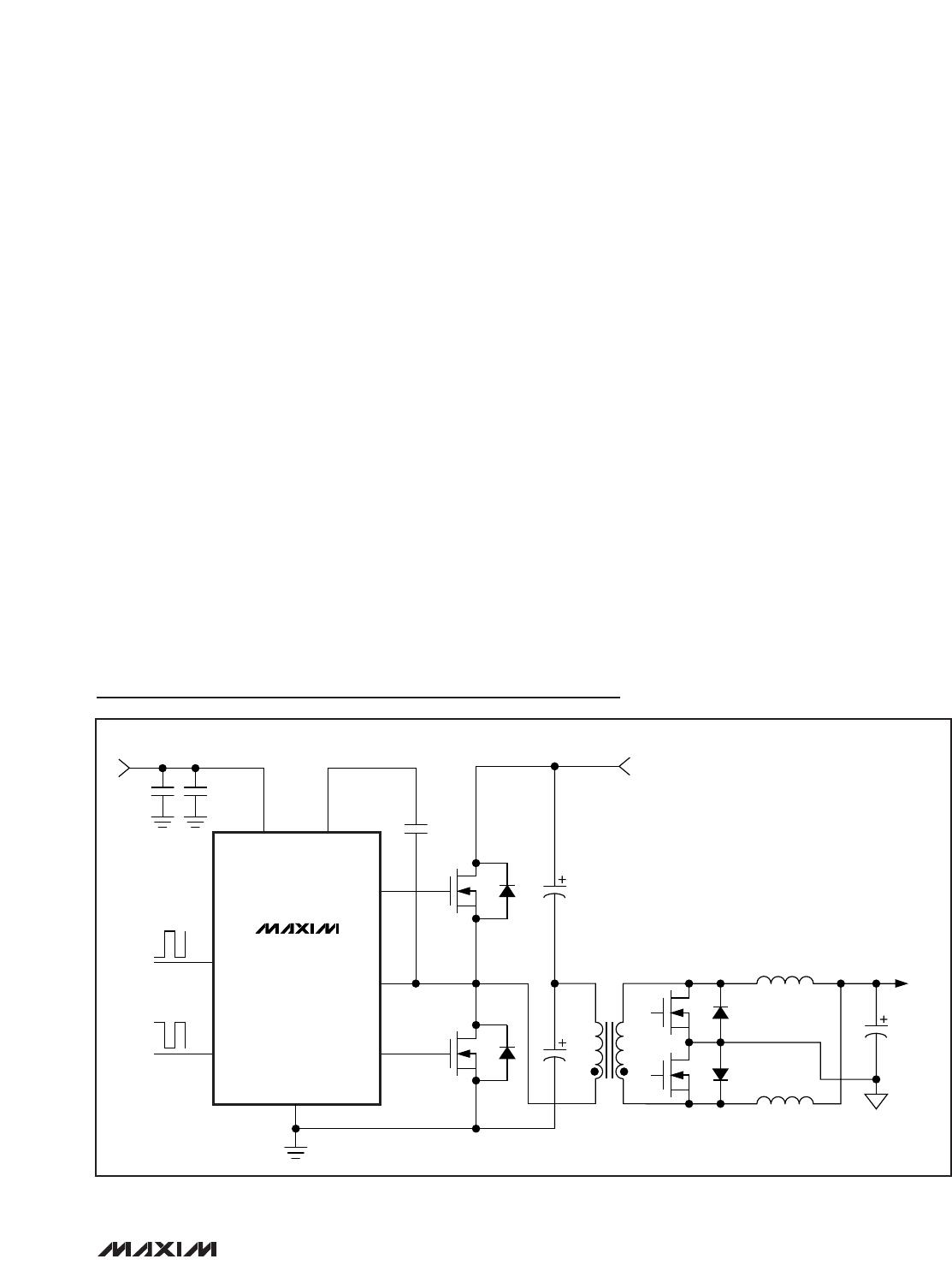
Applications Information
Supply Bypassing and Grounding
Careful attention is required when choosing the bypass-
ing and grounding scheme of the MAX15018_/
MAX15019_. Peak supply and output currents may
exceed 6A when both drivers are simultaneously driving
large external capacitive loads in phase. Supply drops
and ground shifts create forms of negative feedback for
inverterting topologies and may degrade the delay and
transition times. Ground shifts due to insufficient device
grounding may also disturb other circuits sharing the
same AC ground return path. Any series inductance in
the V
DD
, DH, DL, and/or GND paths can cause oscilla-
tions due to the very high di/dt when switching the
MAX15018_/MAX15019_ with any capacitive load. Place
one or more 0.1µF ceramic capacitors in parallel from
V
DD
to GND as close as possible to the device to
bypass the input supply. Use a ground plane to minimize
ground return resistance and series inductance. Place
the external MOSFETs as close as possible to the
MAX15018_/MAX15019_ to reduce trace length and fur-
ther minimize board inductance and AC path resistance.
Power Dissipation
Power dissipation in the MAX15018_/MAX15019_ is pri-
marily due to power loss in the internal boost diode and
the internal nMOS and pMOS FETS. For capacitive
loads, the total power dissipation for the device is:
P
D
= (C
L
x V
DD
2
x f
SW
) + (I
VDDO
+ I
BSTO
) x V
DD
where C
L
is the combined capacitive load at DH and
DL, V
DD
is the supply voltage, and f
SW
is the switching
frequency of the IC. P
D
includes the power dissipated in
the internal bootstrap diode (P
DIODE
). The internal
power dissipation reduces by P
DIODE
, if an external
bootstrap Schottky diode is used. The power dissipation
in the internal boost diode (when driving a capacitive
load) will be the charge through the diode per switching
period multiplied by the maximum diode forward voltage
drop (V
F
= 1V) as given in the following equation.
P
DIODE
= C
DH
x (V
DD
- 1) x f
SW
x V
F
where C
DH
is the capacitive load at DH, V
DD
is the sup-
ply voltage, f
SW
is the switching frequency of the con-
verter, V
F
is the maximum diode forward voltage drop.
The total power dissipation when using the internal
boost diode will be P
D
and, when using an external
Schottky diode, will be P
D
- P
DIODE
. The total power
dissipated in the device must be kept below the maxi-
mum of 1.95W for the 8-pin SO with exposed pad at T
A
= +70°C ambient.
125V/3A, High-Speed,
Half-Bridge MOSFET Drivers
10 ______________________________________________________________________________________