Parameter
Symbol
Unit
Repetitive peak reverse voltage
Continuous reverse voltage
RMS voltage
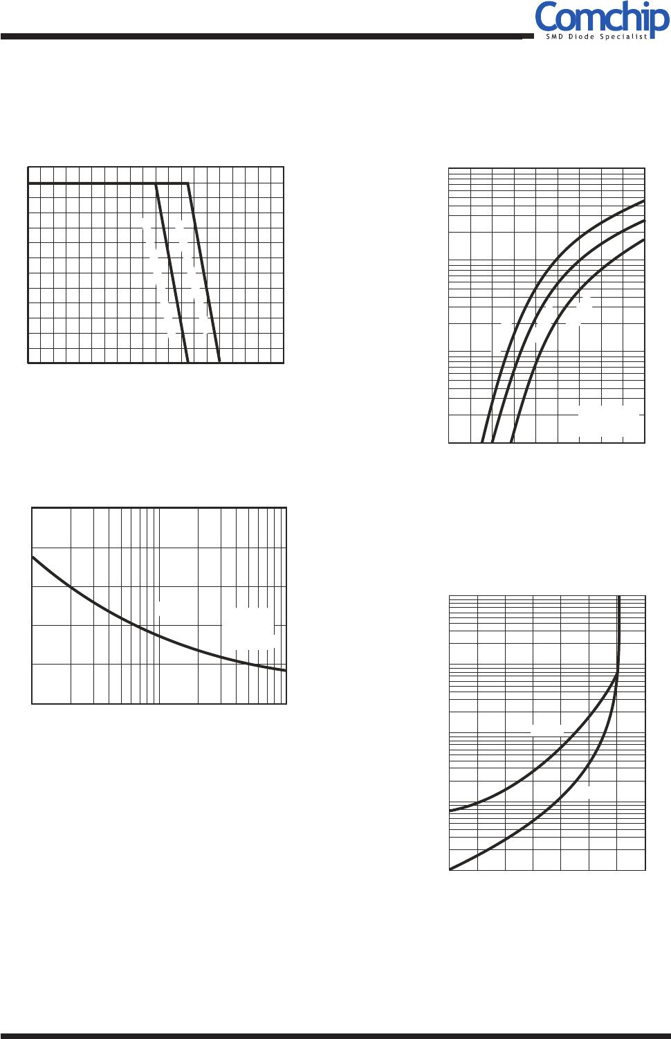
Forward rectified current (See fig. 1)
Maximum forward voltage
IF=6.0A
Forward surge current, 8.3ms single
half sine-wave superimposed on rated
load (JEDEC method)
VR=VRRM TA=25°C
Thermal resistance
Junction to case
Reverse current
TA=100°CVR=VRRM
Page 1
QW-BB032
Chip Schottky Barrier Rectifier
REV:A
Comchip Technology CO., LTD.
VRRM
VR
VRMS
IO
VF
IFSM
IR
RθJA
TJ
620-G
20
20
14
40
40
28
60
60
42
6.0
0.75
75
0.5
20
80
80
80
56
100
100
70
V
V
V
A
V
A
mA
°C/W
°C
0.55 0.85
Operating temperature
Storage temperature
TSTG
-65 to +175
°C
-55 to +125 -55 to +150
3.0
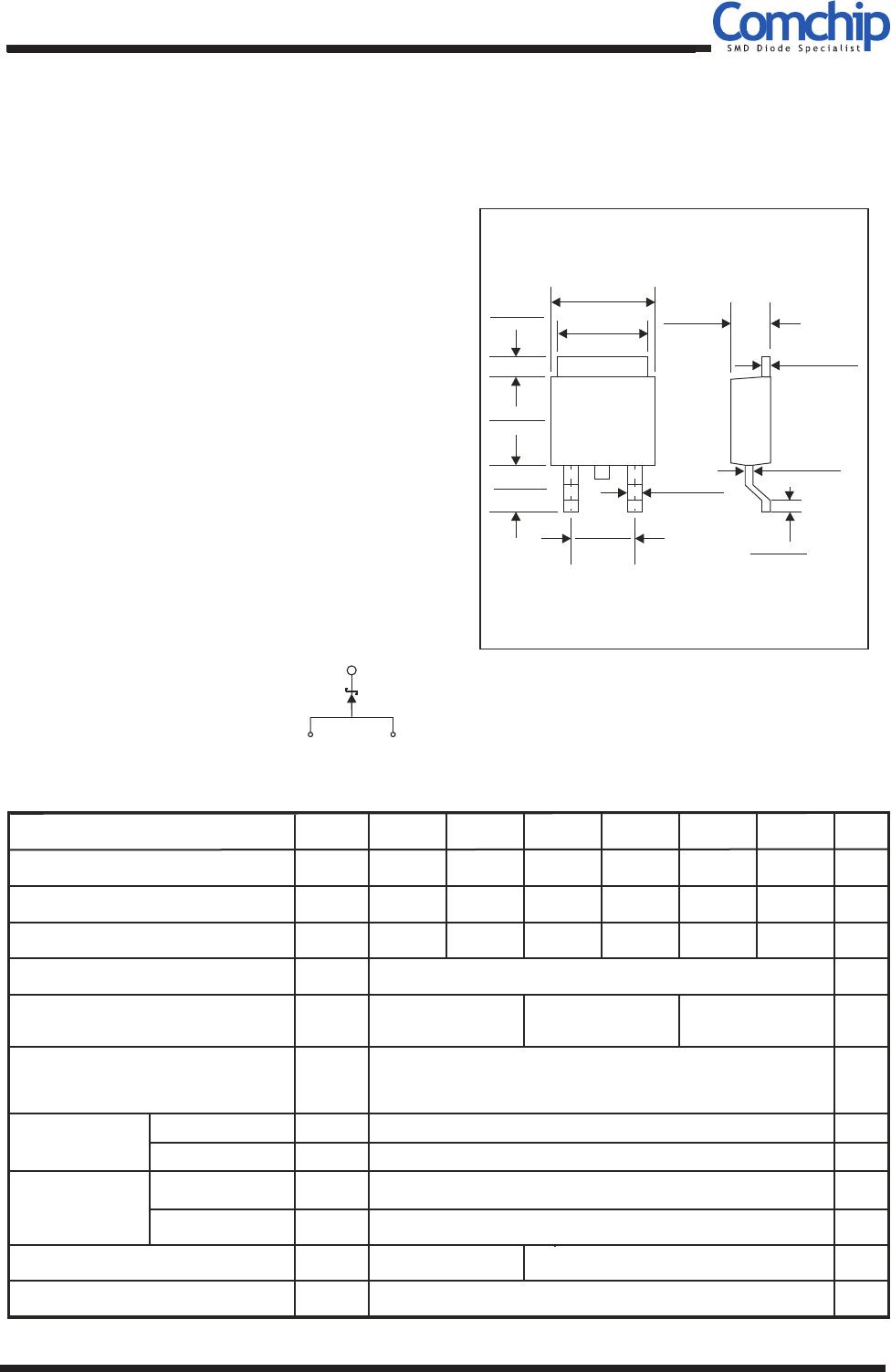
Features
1
3
2=4
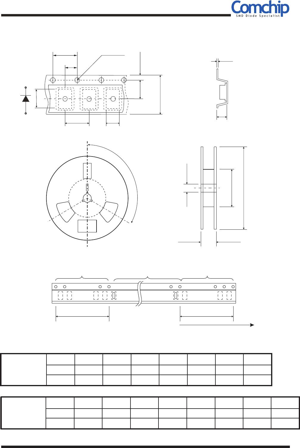
Dimensions in inches and (millimeters)
DPAK
0.217(5.50)
0.201(5.10)
0.264(6.70)
0.248(6.30)
0.114(2.90)
0.098(2.50)
0.244(6.20)
0.228(5.80)
0.048(1.20)
0.031(0.80)
0.185(4.70)
0.169(4.30)
0.039(1.00)
0.031(0.80)
0.024(0.60)
0.016(0.40)
0.024(0.60)
0.016(0.40)
0.098(2.50)
0.083(2.10)
0.032(0.80)
0.016(0.40)
Reverse Voltage: 20 to 100 Volts
Forward Current: 6.0 Amp
RoHS Device
CDBD620-G Thru. CDBD6100-G
Mechanical data
Case: TO-252/DPAK, molded plastic.-
Terminals: solderable per MIL-STD-750, -
method 2026.
Polarity: Indicated by cathode band.-
-Weight:0.34 gram(approx.).
Weunting Position: Any-
Maximum Ratings (At Ta=25°C, unless otherwise noted)
CDBD
640-G
CDBD
650-G
CDBD
660-G
CDBD
680-G
CDBD
6100-G
CDBD
50
50
35
RθJC
Junction to ambient
°C/W
-Batch process design, excellent power dissipation offers
better reverse leakage current and thermal resistance.
-Low profile surface mounted application in order to
optimize board space.
-Low power loss, high efficiency.
-High current capability, low forward voltage drop.
-High surge capability.
-Guardring for overvoltage protection.
-Ultra high-speed switching.
-Silicon epitaxial planar chip, metal silicon junction.
-Lead-free parts meet environmental standards of
MIL-STD-19500 /228
IR mA