Dual-Channel Digital Isolators, 5 kV
Data Sheet
ADuM2210/ADuM2211
Rev. F Document Feedback
Information furnished by Analog Devices is believed to be accurate and reliable. However, no
responsibility is assumed by Analog Devices for its use, nor for any infringements of patents or other
rights of third parties that may result from its use. Specifications subject to change without notice. No
license is granted by implication or otherwise under any patent or patent rights of Analog Devices.
Trademarks and registered trademarks are the property of their respective owners.
One Technology Way, P.O. Box 9106, Norwood, MA 02062-9106, U.S.A.
Tel: 781.329.4700 ©2010–2015 Analog Devices, Inc. All rights reserved.
Technical Support www.analog.com
FEATURES
High isolation voltage: 5000 V rms
Enhanced system-level ESD performance per IEC 61000-4-x
Low power operation
5 V operation
1.6 mA per channel maximum at 0 Mbps to 1 Mbps
3.7 mA per channel maximum at 10 Mbps
3.3 V operation
1.4 mA per channel maximum at 0 Mbps to 1 Mbps
2.4 mA per channel maximum at 10 Mbps
Bidirectional communication
3.3 V/5 V level translation
High temperature operation: 125°C
Default low output
High data rate: dc to 10 Mbps (NRZ)
Precise timing characteristics
3 ns maximum pulse width distortion
3 ns maximum channel-to-channel matching
High common-mode transient immunity: >25 kV/μs
16-lead SOIC wide body package version (RW-16)
16-lead SOIC wide body enhanced creepage version (RI-16)
Safety and regulatory approvals (RI-16 package)
UL recognition: 5000 V rms for 1 minute per UL 1577
CSA Component Acceptance Notice 5A
IEC 60601-1: 250 V rms (reinforced)
IEC 60950-1: 400 V rms (reinforced)
VDE Certificate of Conformity
DIN V VDE V 0884-10 (VDE V 0884-10):2006-12
V
IORM
= 846 V peak
Qualified for automotive applications
APPLICATIONS
General-purpose, high voltage, multichannel isolation
Medical equipment
Power supplies
RS-232/RS-422/RS-485 transceiver isolation
Hybrid electric vehicles, battery monitors, and motor drives
GENERAL DESCRIPTION
The ADuM2210/ADuM2211
1
are 2-channel digital isolators
based on Analog Devices, Inc., iCoupler® technology. Combining
high speed CMOS and monolithic air core transformer technology,
these isolation components provide outstanding performance
characteristics that are superior to alternatives such as optocoupler
devices.
By avoiding the use of LEDs and photodiodes, iCoupler devices
remove the design difficulties commonly associated with optocouplers.
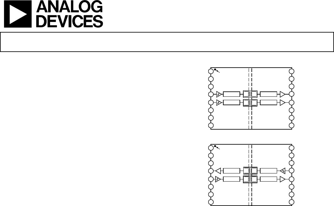
FUNCTIONAL BLOCK DIAGRAMS
1
2
3
4
5
6
7
8
GND
1
NC
V
DD1
V
IA
V
IB
NC
GND
1
NC
GND
2
NC
V
DD2
V
OA
V
OB
NC
NC
GND
2
NC = NO CONNECT
ADuM2210
16
15
14
13
12
11
10
9
ENCODE
ENCODE
DECODE
DECODE
PIN 1
INDICATOR
09233-001
Figure 1.
ADuM2210
1
2
3
4
5
6
7
8
GND
1
NC
V
DD1
V
OA
V
IB
NC
GND
1
NC
GND
2
NC
V
DD2
V
IA
V
OB
NC
NC
GND
2
NC = NO CONNECT
ADuM2211
16
15
14
13
12
11
10
9
DECODE
ENCODE
ENCODE
DECODE
PIN 1
INDICATOR
09233-002
Figure 2.
ADuM2211
Typical optocoupler concerns regarding uncertain current
transfer ratios, nonlinear transfer functions, and temperature
and lifetime effects are eliminated with the simple iCoupler digital
interfaces and stable performance characteristics. The need for
external drivers and other discrete components is eliminated with
these iCoupler products. Furthermore, iCoupler devices run at
one-tenth to one-sixth the power of optocouplers at comparable
signal data rates.
The ADuM2210/ADuM2211 isolators provide two independent
isolation channels in a variety of channel configurations and
data rates (see the Ordering Guide). They operate with the
supply voltage of either side ranging from 3.0 V to 5.5 V, providing
compatibility with lower voltage systems as well as enabling voltage
translation functionality across the isolation barrier. The
ADuM2210W and ADuM2211W are automotive grade versions.
Similar to the ADuM3200/ADuM3201 isolators, the ADuM2210/
ADuM2211 isolators contain various circuit and layout
enhancements to provide increased capability relative to system-
level IEC 61000-4-x testing (ESD, burst, and surge). The precise
capability in these tests for either the ADuM3200/ ADuM3201 or
ADuM2210/ADuM2211 products is strongly determined by the
design and layout of the user’s board or module. For more
information, see the AN-793 Application Note, ESD/Latch-Up
Considerations with iCoupler Isolation Products.
1
Protected by U.S. Patents 5,952,849; 6,873,065; 6,903,578; and 7,075,329. Other patents pending.
ADuM2210/ADuM2211 Data Sheet
Rev. F | Page 2 of 17
TABLE OF CONTENTS
Features .............................................................................................. 1
Applications ....................................................................................... 1
General Description ......................................................................... 1
Functional Block Diagrams ............................................................. 1
Revision History ............................................................................... 2
Specifications ..................................................................................... 3
Electrical Characteristics5 V Operation................................ 3
Electrical Characteristics3.3 V Operation ............................ 4
Electrical CharacteristicsMixed 5 V/3.3 V Operation ........ 5
Electrical CharacteristicsMixed 3.3 V/5 V Operation ........ 6
Package Characteristics ............................................................... 7
Regulatory Information ............................................................... 7
Insulation and Safety-Related Specifications ............................ 7
DIN V VDE V 0884-10 (VDE V 0884-10) Insulation
Characteristics .............................................................................. 8
Recommended Operating Conditions .......................................8
Absolute Maximum Ratings ............................................................9
ESD Caution...................................................................................9
Pin Configurations and Function Descriptions ......................... 10
Typical Performance Characteristics ........................................... 12
Applications Information .............................................................. 13
PCB Layout ................................................................................. 13
Propagation Delay-Related Parameters ................................... 13
DC Correctness and Magnetic Field Immunity ..................... 13
Power Consumption .................................................................. 14
Insulation Lifetime ..................................................................... 15
Outline Dimensions ....................................................................... 16
Ordering Guide .......................................................................... 17
Automotive Products ................................................................. 17
REVISION HISTORY
9/15Rev. E to Rev. F
Changed 3 V Operation to 3.3 V Operation .............. Throughout
Changes to Features Section............................................................ 1
Changes to Table 2 and Table 3 ....................................................... 3
Changes to Table 5 and Table 6 ....................................................... 4
Changes to Table 8 and Table 9 ....................................................... 5
Changes to Table 11 and Table 12 .................................................. 6
3/15Rev. D to Rev. E
Changed ADuM221x to ADuM2210/ADuM2211....... Throughout
Changed ADuM320x to ADuM3200/ADuM3201....... Throughout
Changes to Table 15 .......................................................................... 7
8/12Rev. C to Rev. D
Changes to Table 4 and Table 6 ....................................................... 4
Changes to Table 7 and Table 9 ....................................................... 5
Changes to Table 10 and Table 12 .................................................. 6
Updated Outline Dimensions ....................................................... 16
Changes to Ordering Guide .......................................................... 17
6/12Rev. B to Rev. C
Changes to Features Section, Applications Section, and General
Description Section .......................................................................... 1
Changes to Table 1; Added Table 2 and Table 3, Renumbered
Sequentially ....................................................................................... 3
Changes to Table 4; Added Table 5 and Table 6 ........................... 4
Changed Electrical CharacteristicsMixed 5 V/3 V or 3 V/5 V
Operation Section to Electrical CharacteristicsMixed 5 V/3 V
Operation Section.............................................................................. 5
Changes to Table 7; Added Table 8 and Table 9 ............................ 5
Added Electrical CharacteristicsMixed 3 V/5 V Operation,
Section, Table 10, Table 11, and Table 12 ....................................... 6
Changes to Table 19 ....................................................................... 12
Changes to Ordering Guide .......................................................... 20
Added Automotive Products Section .......................................... 20
2/12Rev. A to Rev. B
Created Hyperlink for Safety and Regulatory Approvals Entry
in Features Section ............................................................................ 1
Change to PCB Layout Section ..................................................... 16
Updated Outline Dimensions ....................................................... 19
8/11Rev. 0 to Rev. A
Added 16-Lead SOIC_IC Package ................................... Universal
Changes to Features Section ............................................................ 1
Changes to Table 5 and Table 6..................................................... 10
Changes to Endnote 1, Table 8...................................................... 11
Updated Outline Dimensions ....................................................... 19
Changes to Ordering Guide .......................................................... 20
9/10Revision 0: Initial Version
Data Sheet ADuM2210/ADuM2211
Rev. F | Page 3 of 17
SPECIFICATIONS
ELECTRICAL CHARACTERISTICS5 V OPERATION
All voltages are relative to their respective ground. 4.5 V ≤ V
DD1
≤ 5.5 V, 4.5 V ≤ V
DD2
5.5 V. All minimum/maximum specifications apply over
the entire recommended operation range, 40°C ≤ T
A
≤ 125°C, unless otherwise noted. All typical specifications are at T
A
= 25°C, V
DD1
=
V
DD2
= 5 V.
Table 1.
Parameter Symbol
S Grade T Grade
Unit Test Conditions/Comments Min Typ Max Min Typ Max
SWITCHING SPECIFICATIONS
Pulse Width PW 1000 100 ns Within PWD limit
Data Rate 1 10 Mbps Within PWD limit
Propagation Delay t
PHL
, t
PLH
20 150 20 50 ns 50% input to 50% output
Pulse Width Distortion PWD 40 3 ns |t
PLH
− t
PHL
|
Change vs. Temperature
5
ps/°C
Propagation Delay Skew t
PSK
100 15 ns Between any two units
Channel Matching
Codirectional t
PSKCD
50 3 ns
Opposing-Direction t
PSKOD
50 17 ns
Table 2.
Parameter Symbol
1 Mbps, S Grade 10 Mbps, T Grade
Unit Test Conditions/Comments Min Typ Max Min Typ Max
SUPPLY CURRENT No load
ADuM2210 I
DD1
1.3 1.7 3.5 4.8 mA
I
DD2
1.0 1.6 1.7 2.8 mA
ADuM2211 I
DD1
1.1 1.5 2.6 4.0 mA
I
DD2
1.3 1.8 3.1 4.1 mA
Table 3.
Parameter Symbol Min Typ Max Unit Test Conditions/Comments
1
DC SPECIFICATIONS
Logic High Input Threshold V
IH
0.7V
DDX
V
Logic Low Input Threshold V
IL
0.3V
DDX
V
Logic High Output Voltages V
OH
V
DDX
− 0.1 5.0 V I
Ox
= −20 µA, V
Ix
= V
IxH
V
DDX
− 0.5 4.8 V I
Ox
= −3.2 mA, V
Ix
= V
IxH
Logic Low Output Voltages V
OL
0.0 0.1 V I
Ox
= 20 µA, V
Ix
= V
IxL
0.2 0.4 V I
Ox
= 3.2 mA, V
Ix
= V
IxL
Input Current per Channel I
I
−10 +0.01 +10 µA 0 V V
IX
V
DDX
Quiescent Input Supply Current I
DDI (Q)
0.4 0.8 mA
Quiescent Output Supply Current I
DDO (Q)
0.5 0.6 mA
Dynamic Input Supply Current I
DDI (D)
0.19 mA/Mbps
Dynamic Output Supply Current I
DDO (D)
0.05 mA/Mbps
AC SPECIFICATIONS
Output Rise/Fall Time t
R
/t
F
ADuM2210/ADuM2211 S Grade 10 ns 10% to 90%
ADuM2210/ADuM2211 T Grade 2.5 ns 10% to 90%
Common-Mode Transient Immunity
2
|CM| 25 35 kV/µs V
Ix
= V
DDX
, V
CM
= 1000 V,
transient magnitude = 800 V
Refresh Period T
r
1.6 µs
1
I
Ox
is the Channel x output current, where x = A or B, V
IxH
is the input side logic high, and V
IxL
is the input side logic low.
2
|CM| is the maximum common-mode voltage slew rate that can be sustained while maintaining V
O
> 0.8 V
DDx
. The common-mode voltage slew rates apply to both
rising and falling common-mode voltage edges.

ADUM2210TRWZ

Mfr. #:
Manufacturer:
Analog Devices Inc.
Description:
Digital Isolators Dual-CH Digital 5kV
Lifecycle:
New from this manufacturer.
Delivery:
DHL FedEx Ups TNT EMS
Payment:
T/T Paypal Visa MoneyGram Western Union