XC17V00 Series Configuration PROMs
DS073 (v1.12) November 13, 2008 www.xilinx.com
Product Specification 3
R
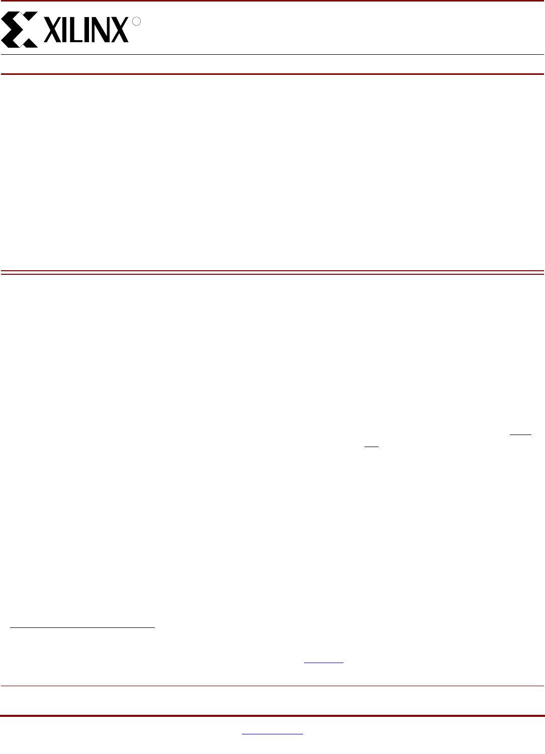
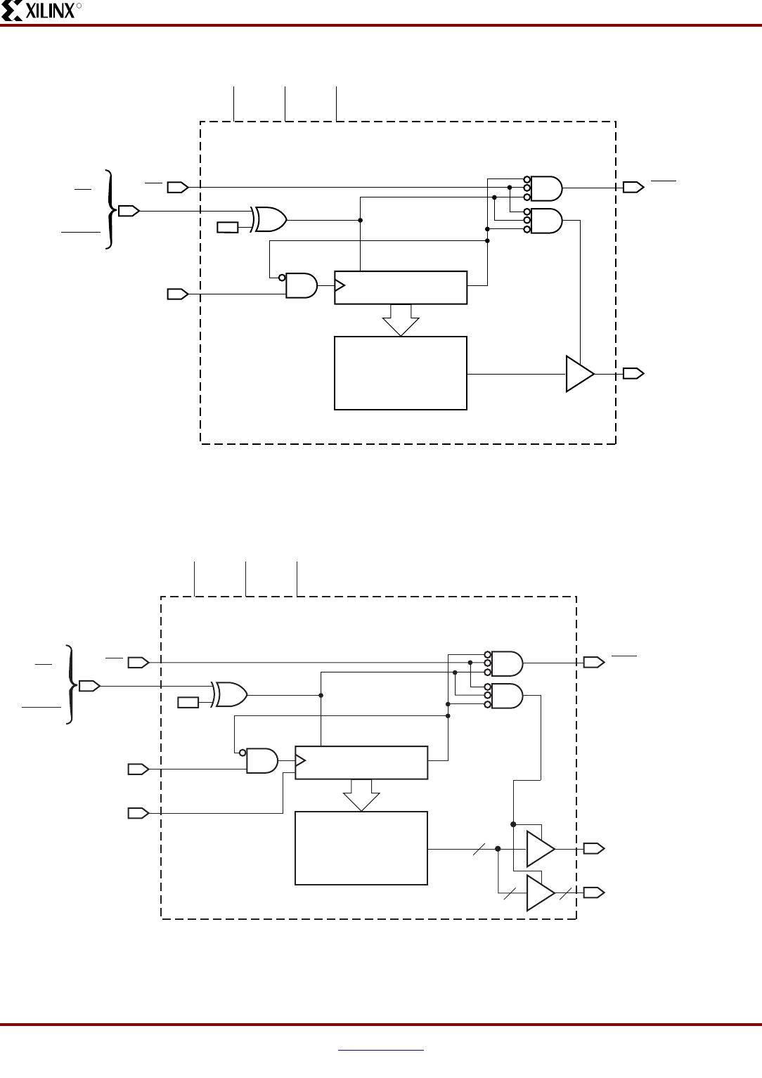
Pin Description
DATA[0:7]
The array data value corresponding to the internal address
counter location is output on enabled DATA[0-7] output
pin(s) when CE
is active, OE is active, and the internal
address counter has not incremented beyond its Terminal
Count (TC) value. Otherwise, all data pins are in a high
impedance state when CE
is inactive, OE is inactive, or the
internal address counter has incremented beyond its
Terminal Count (TC) value.
The XC17V01, XC17V02, and XC17V04 have only the
single DATA output pin for connection to the FPGA serial
configuration data input pin.
The XC17V08 and XC17V16 have the D[0-7] output pins.
During device programming, the XC17V08 and XC17V16
must be programmed for use in either serial output mode or
parallel output mode. For XC17V08 and XC17V16 devices
programmed to serial output mode, only the D0 pin is
enabled for data output to the Virtex
®
series FPGA serial
configuration data input pin. In serial mode, the D[1-7]
output pins remain in high impedance state and may be
unconnected. For XC17V08 and XC17V16 devices
programmed to parallel output mode, all D[0-7] output pins
are enabled for byte-wide data output to the FPGA
SelectMAP configuration data input pins.
The DATA/D0 pin is a bidirectional I/O during device
programming.
CLK
Each rising edge on the CLK input increments the internal
address counter, when CE
is active, OE is active, the
internal address counter has not incremented past its
Terminal Count (TC) value, and BUSY is Low.
Note:
The BUSY condition applies to only the XC17V08 and
XC17V16.
RESET/OE
The polarity of this input pin is programmable as either
RESET/OE
or OE/RESET. The polarity is set at the time of
device programming. The device default is active-High
RESET, but compatibility with Xilinx FPGAs requires the
polarity to be programmed with an active-Low RESET.
When RESET is active, the address counter is held at “0”,
and puts the DATA output in a high-impedance state.
CE
When High, this pin holds the internal address counter in
reset, puts the DATA output in a high-impedance state, and
forces the device into low-I
CC
standby mode.
CEO
Chip Enable Output is connected to the CE input of the next
PROM in the daisy chain. This output is Low when the CE
and OE
inputs are both active AND the internal address
counter has been incremented beyond its Terminal Count
(TC) value. CEO
returns to High when OE goes inactive or
CE
goes High.
BUSY (XC17V16 and XC17V08 Only)
Asserting the BUSY input High prevents rising edges on
CLK from incrementing the internal address counter and
maintains current data on the data pins.
Note:
If the BUSY pin is floating, then the programmable option
to internally tie BUSY to an internal pull-down resistor must be set
during device programming.
V
PP
Programming voltage. No overshoot above the specified
maximum voltage is permitted on this pin. For normal read
operation, this pin must be connected to V
CC
. Failure to do
so may lead to unpredictable, temperature-dependent
operation and severe problems in circuit debugging.
Caution! Do not leave V
PP
floating!
V
CC
and GND
Positive supply and ground pins.
PROM Pinouts for XC17V16 and XC17V08
Pins not listed in Table 1 are “no connect.”
Tabl e 1 : Pinouts for XC17V16 and XC17V08
(1)
Pin Name 44-pin VQFP (VQ44) 44-pin PLCC (PC44)
BUSY 24 30
D0 40 2
D1 29 35
D2 42 4
D3 27 33
D4 9 15
D5 25 31
D6 14 20
D7 19 25
CLK 43 5
RESET/OE
(OE/RESET)
13 19
CE
15 21
GND 6, 18, 28, 37, 41 3, 12, 24, 34, 43
CEO 21 27