XC17V00 Series Configuration PROMs
DS073 (v1.12) November 13, 2008 www.xilinx.com
Product Specification 15
R
Revision History
The following table shows the revision history for this document.
.
Notice of Disclaimer
THE XILINX HARDWARE FPGA AND CPLD DEVICES REFERRED TO HEREIN (“PRODUCTS”) ARE SUBJECT TO THE TERMS AND
CONDITIONS OF THE XILINX LIMITED WARRANTY WHICH CAN BE VIEWED AT http://www.xilinx.com/warranty.htm
. THIS LIMITED
WARRANTY DOES NOT EXTEND TO ANY USE OF PRODUCTS IN AN APPLICATION OR ENVIRONMENT THAT IS NOT WITHIN THE
SPECIFICATIONS STATED IN THE XILINX DATA SHEET. ALL SPECIFICATIONS ARE SUBJECT TO CHANGE WITHOUT NOTICE.
PRODUCTS ARE NOT DESIGNED OR INTENDED TO BE FAIL-SAFE OR FOR USE IN ANY APPLICATION REQUIRING FAIL-SAFE
PERFORMANCE, SUCH AS LIFE-SUPPORT OR SAFETY DEVICES OR SYSTEMS, OR ANY OTHER APPLICATION THAT INVOKES
THE POTENTIAL RISKS OF DEATH, PERSONAL INJURY, OR PROPERTY OR ENVIRONMENTAL DAMAGE (“CRITICAL
APPLICATIONS”). USE OF PRODUCTS IN CRITICAL APPLICATIONS IS AT THE SOLE RISK OF CUSTOMER, SUBJECT TO
APPLICABLE LAWS AND REGULATIONS.
Date Version Revision
07/26/00 1.0 Initial Xilinx release.
10/09/00 1.1 Updated 20-pin PLCC Pinouts.
11/16/00 1.2 Updated pinouts for XC17V16 and XC17V08, I
CCA
DC Characteristic from standby to active mode; C
IN
and C
OUT
from 10 pF to 15 pF, added I
CCS
for XC17V16 and XC17V08 at 500 μA.
02/20/01 1.3 Added note to pinouts for “no connect,” updated Figure 3.
04/04/01 1.4 Added XC2V products to Compatible PROM table, updated Figure 3, updated text for Virtex-II FPGAs.
10/09/01 1.5 Corrected bitstream length for SCV405E, added power-on supply requirements and note for power-on
reset, updated configuration bits for Virtex-II devices, removed CF from Figure 3, and updated FPGA list.
02/27/02 1.6 Added Virtex-II Pro™ FPGAs to the , page 6.
06/14/02 1.7 Made additions and changes to Xilinx FPGAs and Compatible PROMs, page 6.
07/29/02 1.8 Added Virtex-II Pro FPGAs to , page 6.
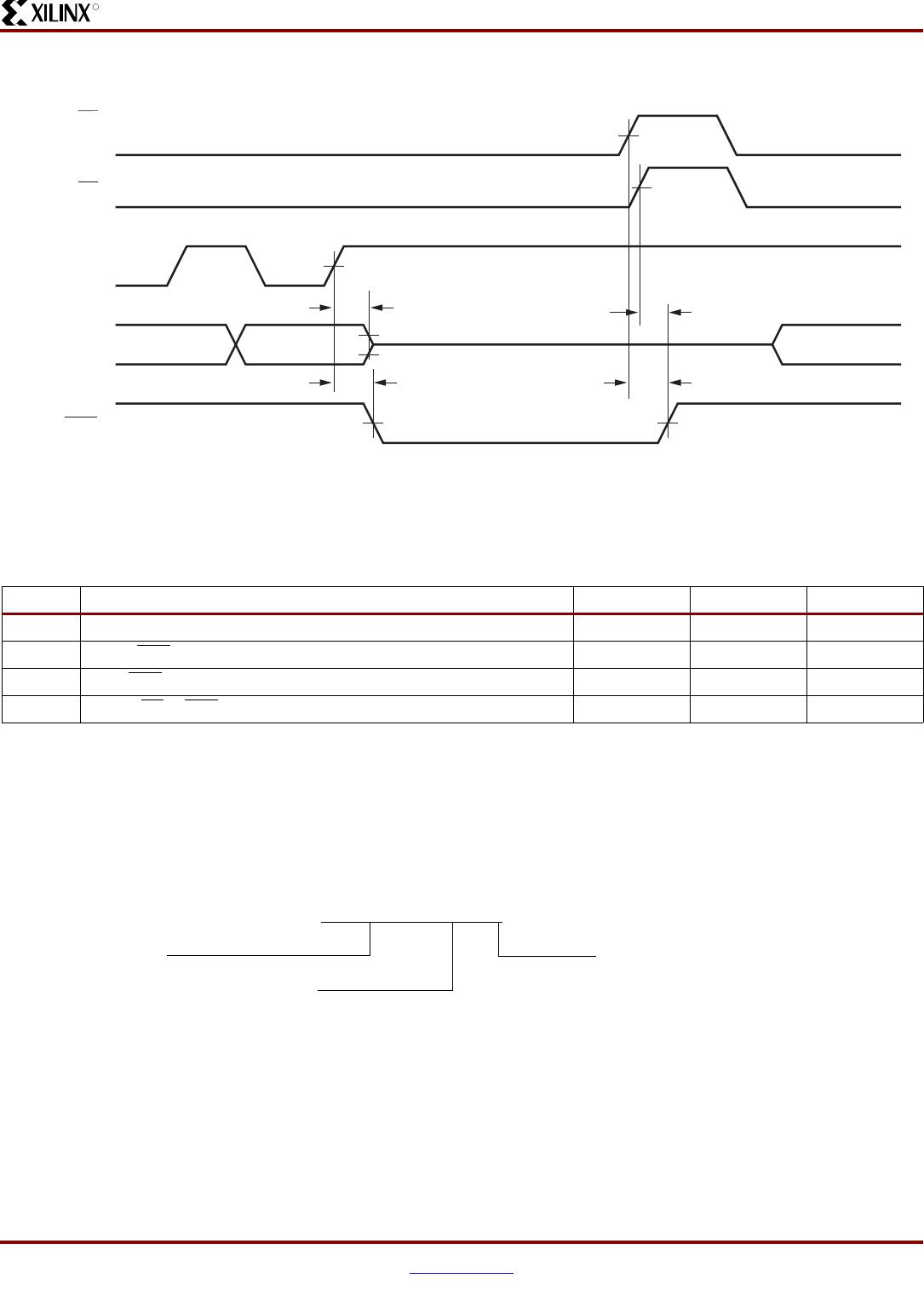
11/05/02 1.9 Added pinout diagrams, changed , page 6, and added footnotes to AC Characteristics over Operating
Condition for XC17V04, XC17V02, and XC17V01, page 11 and AC Characteristics over Operating
Condition for XC17V16 and XC17V08, page 12.
04/10/03 1.10 Added Spartan-3 FPGAs to Truth Table for XC17V00 Control Inputs, page 8.
06/07/07 1.11 • Figure 2, page 2 updated to show correct three-state control on output data buses.
• Corrected XC3S50 bitstream size in Xilinx FPGAs and Compatible PROMs, page 6.
• Added section Selecting Reset Polarity and Configuration Modes, page 7.
• Removed maximum soldering temperature (T
SOL
) from "Absolute Maximum Ratings
(1)
," page 10.
Refer to Xilinx Device Package User Guide for package soldering guidelines.
• Added notes to timing diagram under AC Characteristics over Operating Condition for XC17V04,
XC17V02, and XC17V01, page 11 for clarification.
• Added notes and updated timing diagram AC Characteristics over Operating Condition for XC17V16
and XC17V08, page 12 for clarification.
• Reversed polarity of RESET/OE signal in timing diagram under , page 13 for consistency and added
notes for clarification.
11/13/08 1.12 • Added support for discontinued device and package combinations per XCN07010
.
• Added T
J
to "Absolute Maximum Ratings
(1)
," page 10.
• Updated Figure 3.