CY15B064J
64-Kbit (8K × 8) Serial (I
2
C) Automotive-A
F-RAM
Cypress Semiconductor Corporation 198 Champion Court San Jose, CA 95134-1709 408-943-2600
Document Number: 002-10221 Rev. *B Revised March 24, 2017
64-Kbit (8K × 8) Serial (I
2
C) Automotive-A F-RAM
Features
64-Kbit ferroelectric random access memory (F-RAM) logically
organized as 8K × 8
High-endurance 100 trillion (10
14
) read/writes
151-year data retention (See the Data Retention and
Endurance table)
NoDelay™ writes
Advanced high-reliability ferroelectric process
Fast two-wire Serial interface (I
2
C)
Up to 1-MHz frequency
Direct hardware replacement for serial (I
2
C) EEPROM
Supports legacy timings for 100 kHz and 400 kHz
Low power consumption
100 A (typ) active current at 100 kHz
3 A (typ) standby current
Voltage operation: V
DD
= 2.7 V to 3.65 V
Automotive-A temperature: –40 C to +85 C
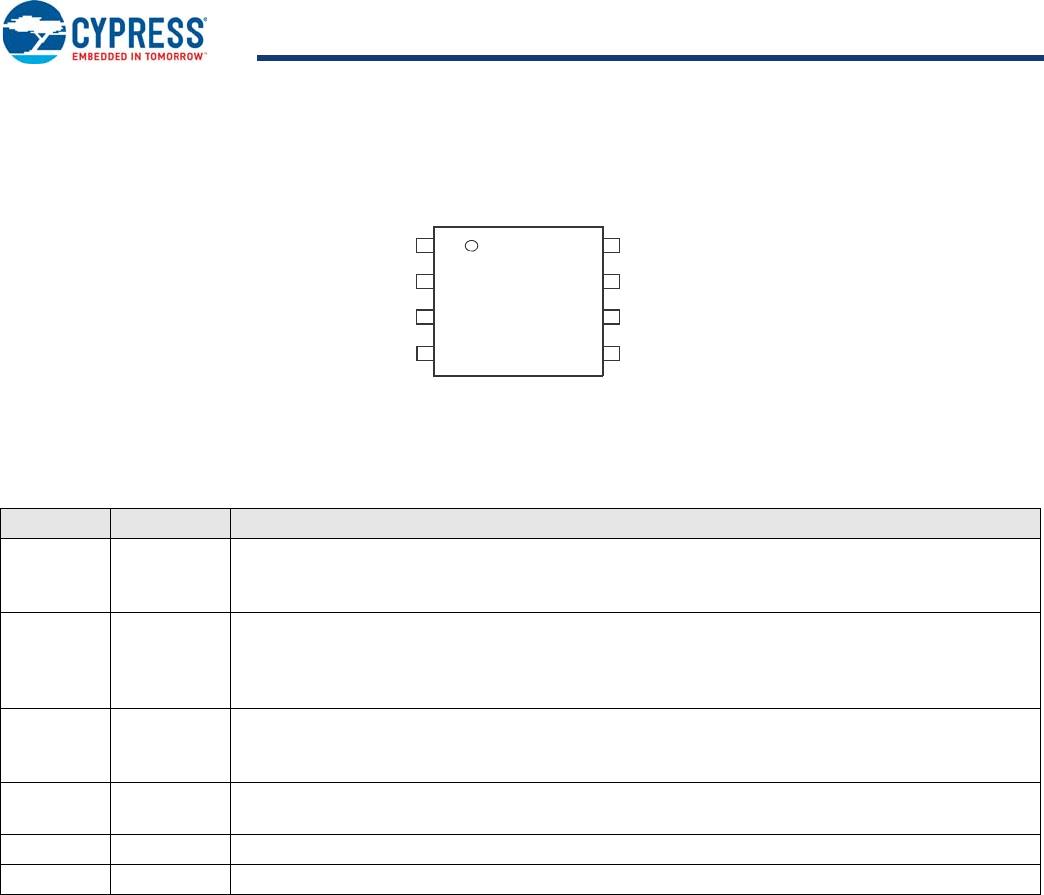
8-pin small outline integrated circuit (SOIC) package
Restriction of hazardous substances (RoHS) compliant
Functional Description
The CY15B064J is a 64-Kbit nonvolatile memory employing an
advanced ferroelectric process. A ferroelectric random access
memory or F-RAM is nonvolatile and performs reads and writes
similar to a RAM. It provides reliable data retention for 151 years
while eliminating the complexities, overhead, and system-level
reliability problems caused by EEPROM and other nonvolatile
memories.
Unlike EEPROM, the CY15B064J performs write operations at
bus speed. No write delays are incurred. Data is written to the
memory array immediately after each byte is successfully
transferred to the device. The next bus cycle can commence
without the need for data polling. In addition, the product offers
substantial write endurance compared with other nonvolatile
memories. Also, F-RAM exhibits much lower power during writes
than EEPROM since write operations do not require an internally
elevated power supply voltage for write circuits. The CY15B064J
is capable of supporting 10
14
read/write cycles, or 100 million
times more write cycles than EEPROM.
These capabilities make the CY15B064J ideal for nonvolatile
memory applications, requiring frequent or rapid writes.
Examples range from data logging, where the number of write
cycles may be critical, to demanding industrial controls where the
long write time of EEPROM can cause data loss. The
combination of features allows more frequent data writing with
less overhead for the system.
The CY15B064J provides substantial benefits to users of serial
(I
2
C) EEPROM as a hardware drop-in replacement. The device
specifications are guaranteed over an automotive-a temperature
range of –40 C to +85 C.
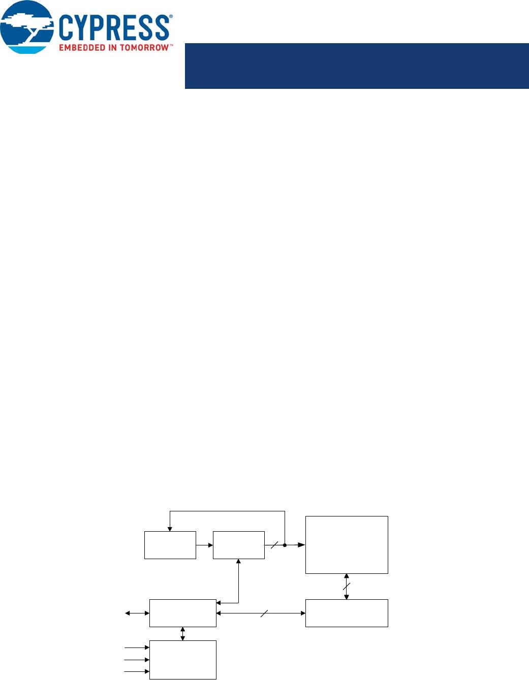
Logic Block Diagram
Address
Latch
8 K x 8
F-RAM Array
Data Latch
8
SDA
Counter
Serial to Parallel
Converter
Control Logic
SCL
WP
A2-A0
13
8
CY15B064J
Document Number: 002-10221 Rev. *B Page 2 of 17
Contents
Pinout ................................................................................3
Pin Definitions ..................................................................3
Functional Overview ........................................................4
Memory Architecture ........................................................4
I2C Interface ......................................................................4
STOP Condition (P) .....................................................4
START Condition (S) ...................................................4
Data/Address Transfer ................................................5
Acknowledge/No-acknowledge ...................................5
Slave Device Address .................................................6
Addressing Overview ..................................................6
Data Transfer ..............................................................6
Memory Operation ............................................................6
Write Operation ...........................................................6
Read Operation ...........................................................7
Endurance .........................................................................8
Maximum Ratings .............................................................9
Operating Range ...............................................................9
DC Electrical Characteristics ..........................................9
Data Retention and Endurance .....................................10
Capacitance ....................................................................10
Thermal Resistance ........................................................10
AC Test Loads and Waveforms .....................................10
AC Test Conditions ........................................................10
AC Switching Characteristics .......................................11
Power Cycle Timing .......................................................12
Ordering Information ......................................................13
Ordering Code Definitions .........................................13
Package Diagram ............................................................14
Acronyms ........................................................................15
Document Conventions .................................................15
Units of Measure .......................................................15
Document History Page .................................................16
Sales, Solutions, and Legal Information ......................17
Worldwide Sales and Design Support ....................... 17
Products ....................................................................17
PSoC® Solutions ......................................................17
Cypress Developer Community .................................17
Technical Support .....................................................17
CY15B064J
Document Number: 002-10221 Rev. *B Page 3 of 17
Pinout
Figure 1. 8-pin SOIC pinout
WP
SCL
1
2
3
4
5
A0
8
7
6
V
DD
SDA
A1
Top View
not to scale
V
SS
A2
Pin Definitions
Pin Name I/O Type Description
A2–A0 Input Device Select Address 2–0. These pins are used to select one of up to 8 devices of the same type
on the same I
2
C bus. To select the device, the address value on the three pins must match the corre-
sponding bits contained in the slave address. The address pins are pulled down internally.
SDA Input/Output Serial Data/Address. This is a bi-directional pin for the I
2
C interface. It is open-drain and is intended
to be wire-AND'd with other devices on the I
2
C bus. The input buffer incorporates a Schmitt trigger for
noise immunity and the output driver includes slope control for falling edges. An external pull-up resistor
is required.
SCL Input Serial Clock. The serial clock pin for the I
2
C interface. Data is clocked out of the device on the falling
edge, and into the device on the rising edge. The SCL input also incorporates a Schmitt trigger input
for noise immunity.
WP Input Write Protect. When tied to V
DD
, addresses in the entire memory map will be write-protected. When
WP is connected to ground, all addresses are write enabled. This pin is pulled down internally.
V
SS
Power supply Ground for the device. Must be connected to the ground of the system.
V
DD
Power supply Power supply input to the device.

CY15B064J-SXA

Mfr. #:
Manufacturer:
Cypress Semiconductor
Description:
F-RAM F-RAM Memory Serial
Lifecycle:
New from this manufacturer.
Delivery:
DHL FedEx Ups TNT EMS
Payment:
T/T Paypal Visa MoneyGram Western Union

Products related to this Datasheet