CY15B064J
Document Number: 002-10221 Rev. *B Page 7 of 17
Read Operation
There are two basic types of read operations. They are current
address read and selective address read. In a current address
read, the CY15B064J uses the internal address latch to supply
the address. In a selective read, the user performs a procedure
to set the address to a specific value.
Current Address & Sequential Read
As mentioned above the CY15B064J uses an internal latch to
supply the address for a read operation. A current address read
uses the existing value in the address latch as a starting place
for the read operation. The system reads from the address
immediately following that of the last operation.
To perform a current address read, the bus master supplies a
slave address with the LSB set to a ‘1’. This indicates that a read
operation is requested. After receiving the complete slave
address, the CY15B064J will begin shifting out data from the
current address on the next clock. The current address is the
value held in the internal address latch.
Beginning with the current address, the bus master can read any
number of bytes. Thus, a sequential read is simply a current
address read with multiple byte transfers. After each byte the
internal address counter will be incremented.
Note Each time the bus master acknowledges a byte, this
indicates that the CY15B064J should read out the next
sequential byte.
There are four ways to properly terminate a read operation.
Failing to properly terminate the read will most likely create a bus
contention as the CY15B064J attempts to read out additional
data onto the bus. The four valid methods are:
1. The bus master issues a no-acknowledge in the 9th clock
cycle and a STOP in the 10th clock cycle. This is illustrated in
the diagrams below. This is preferred.
2. The bus master issues a no-acknowledge in the 9th clock
cycle and a START in the 10th.
3. The bus master issues a STOP in the 9th clock cycle.
4. The bus master issues a START in the 9th clock cycle.
If the internal address reaches 1FFFh, it will wrap around to
0000h on the next read cycle. Figure 9 and Figure 10 below show
the proper operation for current address reads.
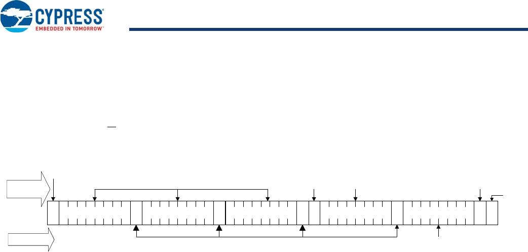
Figure 8. Multi-Byte Write
S ASlave Address 0 Address MSB A Data Byte A P
By Master
By F-RAM
Start
Address & Data
Stop
Acknowledge
Address LSB A Data Byte A
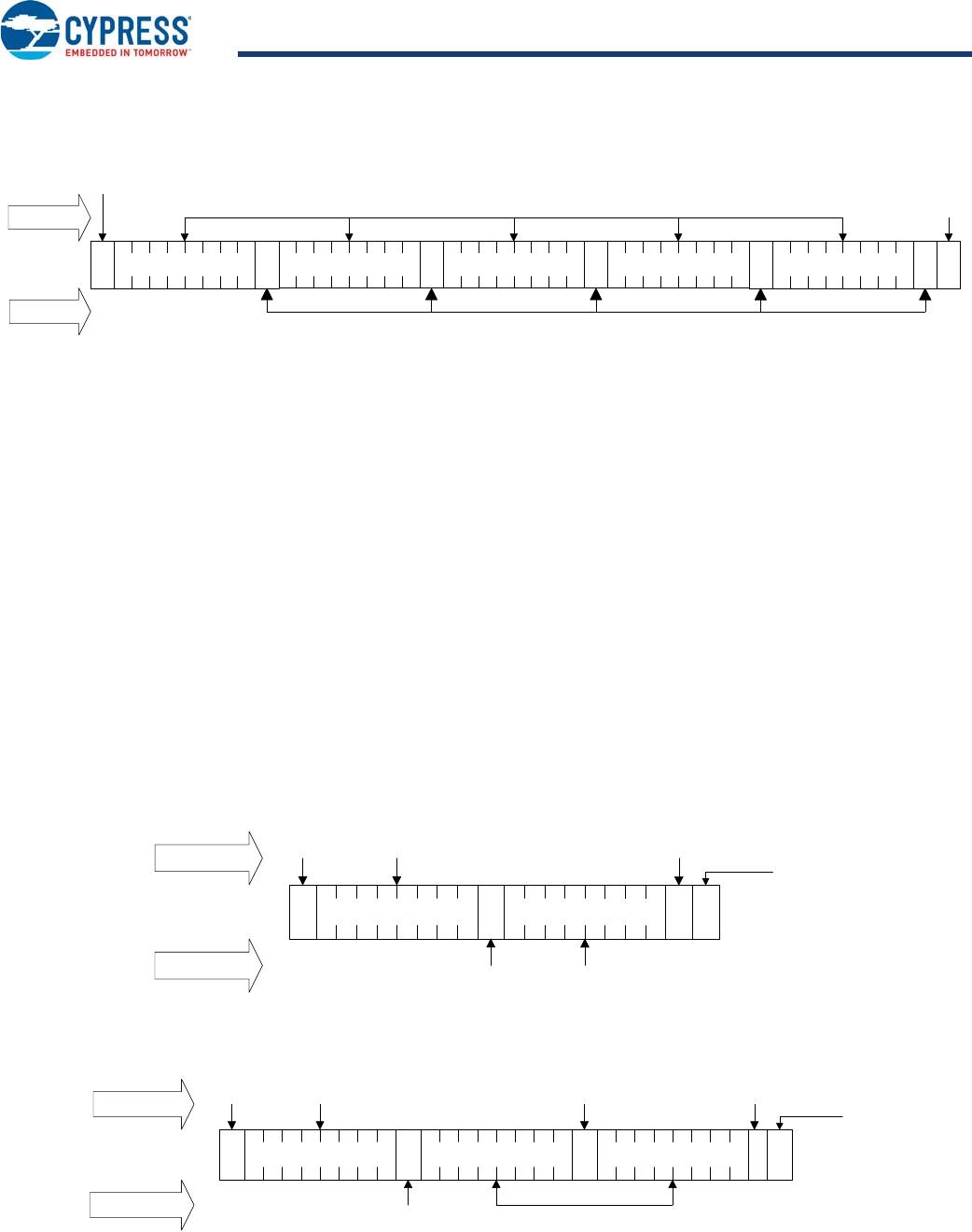
Figure 9. Current Address Read
S ASlave Address 1 Data Byte 1 P
By Master
By F-RAM
Start Address
Stop
Acknowledge
No
Acknowledge
Data
Figure 10. Sequential Read
S ASlave Address 1 Data Byte 1 P
By Master
By F-RAM
Start Address
Stop
Acknowledge
No
Acknowledge
Data
Data ByteA
Acknowledge
CY15B064J
Document Number: 002-10221 Rev. *B Page 8 of 17
Selective (Random) Read
There is a simple technique that allows a user to select a random
address location as the starting point for a read operation. This
involves using the first three bytes of a write operation to set the
internal address followed by subsequent read operations.
To perform a selective read, the bus master sends out the slave
address with the LSB (R/W) set to 0. This specifies a write
operation. According to the write protocol, the bus master then
sends the address bytes that are loaded into the internal address
latch. After the CY15B064J acknowledges the address, the bus
master issues a START condition. This simultaneously aborts
the write operation and allows the read command to be issued
with the slave address LSB set to a '1'. The operation is now a
current address read.
Endurance
The CY15B064J internally operates with a read and restore
mechanism. Therefore, endurance cycles are applied for each
read or write cycle. The memory architecture is based on an
array of rows and columns. Each read or write access causes an
endurance cycle for an entire row. In the CY15B064J, a row is
64 bits wide. Every 8-byte boundary marks the beginning of a
new row. Endurance can be optimized by ensuring frequently
accessed data is located in different rows. Regardless, FRAM
read and write endurance is effectively unlimited at the 1 MHz
I
2
C speed. Even at 3000 accesses per second to the same
segment, 10 years time will elapse before 1 trillion endurance
cycles occur.
Figure 11. Selective (Random) Read
S ASlave Address 1 Data Byte 1 P
By Master
By F-RAM
Start Address
Stop
No
Acknowledge
Data
S ASlave Address 0 Address MSB A
Start
Address
Acknowledge
Address LSB A
CY15B064J
Document Number: 002-10221 Rev. *B Page 9 of 17
Maximum Ratings
Exceeding maximum ratings may shorten the useful life of the
device. These user guidelines are not tested.
Storage temperature ................................ –55 C to +125 C
Maximum accumulated storage time
At 125 °C ambient temperature ................................. 1000 h
At 85 °C ambient temperature ................................ 10 Years
Ambient temperature
with power applied ................................... –55 °C to +125 °C
Supply voltage on V
DD
relative to V
SS
.........–1.0 V to +5.0 V
Input voltage .......... –1.0 V to + 5.0 V and V
IN
< V
DD
+ 1.0 V
DC voltage applied to outputs
in High-Z state ....................................–0.5 V to V
DD
+ 0.5 V
Transient voltage (< 20 ns)
on any pin to ground potential ............–2.0 V to V
DD
+ 2.0 V
Package power
dissipation capability (T
A
= 25 °C) ...............................1.0 W
Surface mount lead
soldering temperature (10 seconds) ........................ +260 C
Electrostatic Discharge Voltage
[1]
Human Body Model (AEC-Q100-002 Rev. E) ..................... 2 kV
Charged Device Model
(AEC-Q100-011 Rev. B) ................500 V
Latch-up current ....................................................> 140 mA
* Exception: The “V
IN
< V
DD
+ 1.0 V” restriction does not apply
to the SCL and SDA inputs.
Operating Range
Range Ambient Temperature (T
A
) V
DD
Automotive-A –40 C to +85 C 2.7 V to 3.65 V
DC Electrical Characteristics
Over the Operating Range
Parameter Description Test Conditions Min Typ
[2]
Max Unit
V
DD
Power supply 2.7 3.3 3.65 V
I
DD
Average V
DD
current SCL toggling
between
V
DD
– 0.3 V and V
SS
,
other inputs V
SS
or
V
DD
– 0.3 V.
f
SCL
= 100 kHz 100 A
f
SCL
= 400 kHz 170 A
f
SCL
= 1 MHz 300 A
I
SB
Standby current SCL = SDA = V
DD
. All
other inputs V
SS
or
V
DD
.
Stop command
issued.
–36A
I
LI
Input leakage current
(Except WP and A2–A0)
V
SS
< V
IN
< V
DD
–1 +1 A
Input leakage current
(for WP and A2–A0)
V
SS
< V
IN
< V
DD
–1 +100 A
I
LO
Output leakage current V
SS
< V
IN
< V
DD
–1 +1 A
V
IH
Input HIGH voltage 0.7 × V
DD
–V
DD
+ 0.3 V
V
IL
Input LOW voltage – 0.3 0.3 × V
DD
V
V
OL
Output LOW voltage I
OL
= 3 mA 0.4 V
R
in
[3]
Input resistance (WP, A2–A0) For V
IN
= V
IL (Max)
40 k
For V
IN
= V
IH (Min)
1––M
V
HYS
[4]
Input hysteresis 0.05 × V
DD
––V
Notes
1. Electrostatic Discharge voltages specified in the datasheet are the AEC-Q100 standard limits used for qualifying the device. To know the maximum value device
passes for, please refer to the device qualification report available on the website.
2. Typical values are at 25 °C, V
DD
= V
DD
(typ). Not 100% tested.
3. The input pull-down circuit is strong (40 k) when the input voltage is below V
IL
and weak (1 M) when the input voltage is above V
IH
.
4. This parameter is guaranteed by design and is not tested.

CY15B064J-SXA

Mfr. #:
Manufacturer:
Cypress Semiconductor
Description:
F-RAM F-RAM Memory Serial
Lifecycle:
New from this manufacturer.
Delivery:
DHL FedEx Ups TNT EMS
Payment:
T/T Paypal Visa MoneyGram Western Union

Products related to this Datasheet