Data Sheet ADuM5400
Rev. B | Page 9 of 16
TYPICAL PERFORMANCE CHARACTERISTICS
Each voltage is relative to its respective ground; all typical specifications are at T
A
= 25°C.
0
5
10
15
20
25
30
35
40
0 0.02 0.04 0.06 0.08 0.10 0.12
OUTPUT CURRENT (A)
EFFICIENCY (%)
5V IN/5V OUT
07509-005
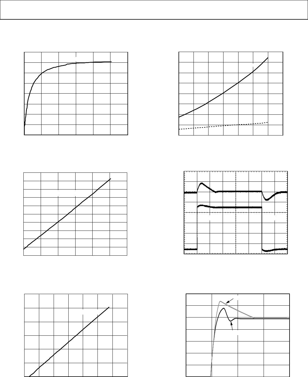
Figure 4. Typical Power Supply Efficiency at 5 V/5 V
0
0.1
0.2
0.3
0.4
0.5
0.6
0.7
0.8
0.9
1.0
0 0.02 0.04 0.06 0.08 0.10 0.12
I
ISO
(A)
POWER DISSIPATION (W)
V
DD1
= 5V, V
ISO
= 5V
07509-006
Figure 5. Typical Total Power Dissipation vs. I
ISO
with Data Channels Idle
0
0.02
0.04
0.06
0.08
0.10
0.12
0 0.05 0.10 0.15 0.20 0.25 0.350.30
INPUT CURRENT (A)
OUTPUT CURRENT (A)
5V IN/5V OUT
07509-007
Figure 6. Typical Isolated Output Supply Current, I
ISO
, as a Function
of External Load, No Dynamic Current Draw at 5 V/5 V
0
0.5
1.0
1.5
2.0
2.5
3.0
3.5
4.0
0
0.5
1.0
1.5
2.0
2.5
3.0
3.5
4.0
3.0 3.5 4.0 4.5 5.0 5.5 6.0 6.5
INPUT VOLTAGE (V)
INPUT CURRENT (A)
POWER (W)
I
DD
POWER
07509-008
Figure 7. Typical Short-Circuit Input Current and Power vs. V
DD1
Supply Voltage
OUTPUT VOLTAGE
(500mV/DIV)
(100µs/DIV)
DYNAMIC LOAD
10% LOAD 90% LOAD
07509-009
Figure 8. Typical V
ISO
Transient Load Response, 5 V Output,
10% to 90% Load Step
TIME (ms)
V
ISO
(V)
7
6
5
4
3
2
1
0
–1 0 1 2 3
90% LOAD
10% LOAD
07509-027
Figure 9. Typical V
ISO
= 5 V Output Voltage Start-Up Transient
at 10% and 90% Load
ADuM5400 Data Sheet
Rev. B | Page 10 of 16
BW = 20MHz (400ns/DIV)
5V OUTPUT RIPPLE (10mV/DIV)
07509-011
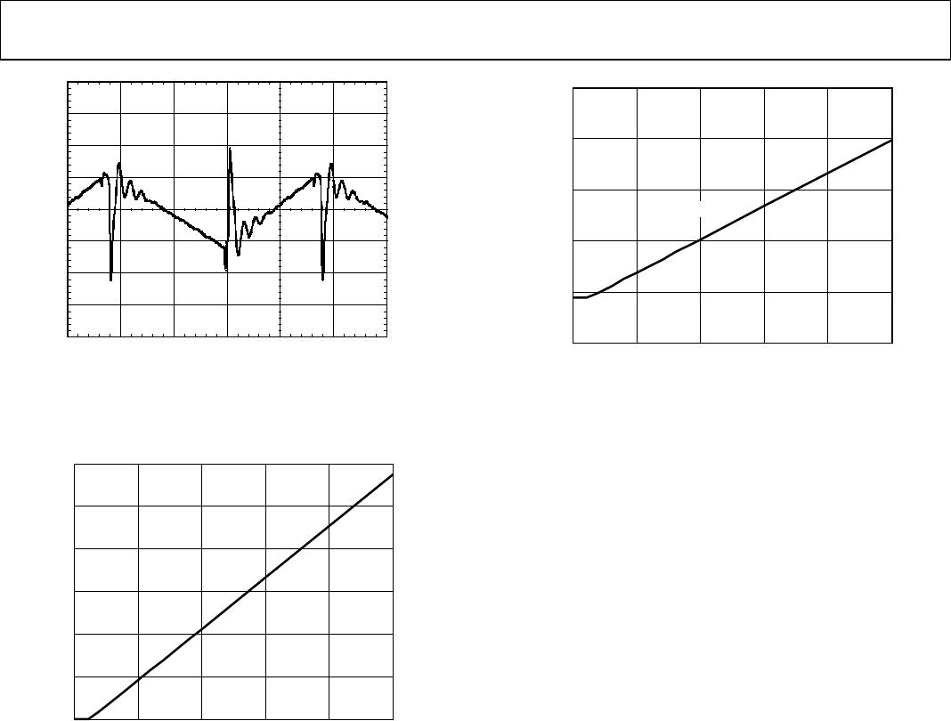
Figure 10. Typical V
ISO
= 5 V Output Voltage Ripple at 90% Load
0
1.0
0.5
1.5
2.0
2.5
3.0
0 5 10 15
DATA RATE (Mbps)
SUPPLY CURRENT (mA)
20 25
5V
07509-016
Figure 11. Typical I
ISO(D)
Dynamic Supply Current per Output
(15 pF Output Load)
0
4
8
12
16
20
0 5 10 15
DATA RATE (Mbps)
SUPPLY CURRENT (mA)
20 25
5V IN/5V OUT
07509-013
Figure 12. Typical I
CH
Supply Current per Forward Data Channel
(15 pF Output Load)
Data Sheet ADuM5400
Rev. B | Page 11 of 16
TERMINOLOGY
I
DD1(Q)
I
DD1(Q)
is the minimum operating current drawn at the V
DD1
pin when there is no external load at V
ISO
and the I/O pins
are operating below 2 Mbps, requiring no additional dynamic
supply current.
I
DD1(MAX)
I
DD1(MAX)
is the input current under full dynamic and V
ISO
load
conditions.
t
PHL
Propagation Delay
t
PHL
propagation delay is measured from the 50% level of the
falling edge of the V
Ix
signal to the 50% level of the falling edge
of the V
Ox
signal.
t
PLH
Propagation Delay
t
PLH
propagation delay is measured from the 50% level of the
rising edge of the V
Ix
signal to the 50% level of the rising edge
of the V
Ox
signal.
Propagation Delay Skew (t
PSK
)
t
PSK
is the magnitude of the worst-case difference in t
PHL
and/or
t
PLH
that is measured between units at the same operating
temperature, supply voltages, and output load within the
recommended operating conditions.
Channel-to-Channel Matching
Channel-to-channel matching is the absolute value of the
difference in propagation delays between two channels when
operated with identical loads.
Minimum Pulse Width
The minimum pulse width is the shortest pulse width at which
the specified pulse width distortion is guaranteed.
Maximum Data Rate
The maximum data rate is the fastest data rate at which the
specified pulse width distortion is guaranteed.
ADUM5400ARWZ

Mfr. #:
Manufacturer:
Analog Devices / Linear Technology
Description:
Digital Isolators Quad-CH w/ Intg DC/DC Converter
Lifecycle:
New from this manufacturer.
Delivery:
DHL FedEx Ups TNT EMS
Payment:
T/T Paypal Visa MoneyGram Western Union

Products related to this Datasheet