ADuM5400 Data Sheet
Rev. B | Page 14 of 16
Note that in the presence of strong magnetic fields and high
frequencies, any loops formed by PCB traces may induce error
voltages sufficiently large to trigger the thresholds of succeeding
circuitry. Exercise care in the layout of such traces to avoid this
possibility.
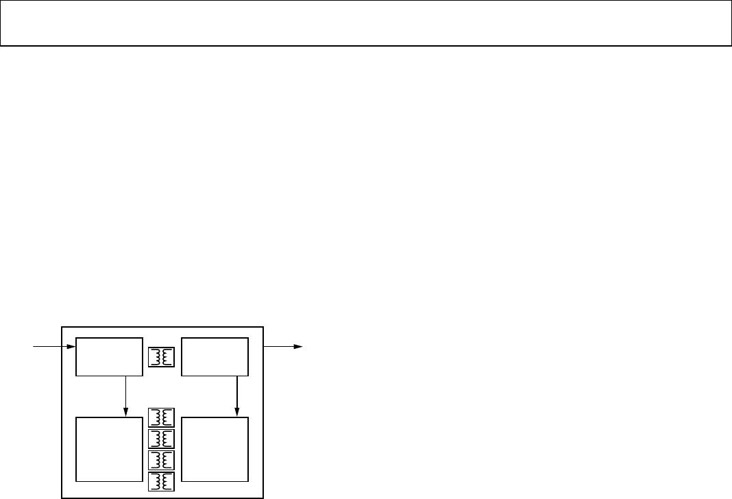
POWER CONSUMPTION
The V
DD1
power supply input provides power to the iCoupler
data channels, as well as to the power converter. For this reason,
the quiescent currents drawn by the data converter and the
primary and secondary I/O channels cannot be determined
separately. All of these quiescent power demands have been
combined into the I
DD1(Q)
current, as shown in Figure 17. The
total I
DD1
supply current is equal to the sum of the quiescent
operating current; the dynamic current due to high data rate,
and any external I
ISO
load.
CONVERTER
PRIMARY
CONVERTER
SECONDARY
PRIMARY
DATA
I/O
4-CHANNEL
I
DDP(D)
SECONDARY
DATA
I/O
4-CHANNEL
I
ISO(D)
I
ISO
I
DD1
7509-021
Figure 17. Power Consumption Within the ADuM5400
Dynamic I/O current is consumed only when operating a channel
at speeds higher than the refresh rate of f
r
. The dynamic current
of each channel is determined by its data rate. Figure 12 shows
the current for a channel in the forward direction, meaning that
the input is on the V
DD1
side of the part.
The following relationship allows the total I
DD1
current to be
calculated:
I
DD1
= (I
ISO
× V
ISO
)/(E × V
DD1
) + Σ I
CHn
; n = 1 to 4 (1)
where:
I
DD1
is the total supply input current.
I
CHn
is the current drawn by a single channel determined from
Figure 12.
I
ISO
is the current drawn by the secondary side external load.
E is the power supply efficiency at 100 mA load from Figure 4
at the V
ISO
and V
DD1
condition of interest.
The maximum external load can be calculated by subtracting
the dynamic output load from the maximum allowable load.
I
ISO(LOAD)
= I
ISO(MAX)
− Σ I
ISO(D)n
; n = 1 to 4 (2)
where:
I
ISO(LOAD)
is the current available to supply an external secondary
side load.
I
ISO(MAX)
is the maximum external secondary side load current
available at V
ISO
.
I
ISO(D)n
is the dynamic load current drawn from V
ISO
by an
output channel, as shown in Figure 11.
The preceding analysis assumes a 15 pF capacitive load on
each data output. If the capacitive load is larger than 15 pF,
the additional current must be included in the analysis of I
DD1
and I
ISO(LOAD)
.
POWER CONSIDERATIONS
The ADuM5400 power input, the data input channels on the
primary side, and the data output channels on the secondary side
are all protected from premature operation by UVLO circuitry.
Below the minimum operating voltage, the power converter holds
its oscillator inactive, and all input channel drivers and refresh
circuits are idle. Outputs are held in a low state to prevent trans-
mission of undefined states during power-up and power-down
operations.
During application of power to V
DD1
, the primary side circuitry
is held idle until the UVLO preset voltage is reached.
The primary side input channels sample the input and send a
pulse to the inactive secondary output. As the secondary side
converter begins to accept power from the primary, the V
ISO
voltage starts to rise. When the secondary side UVLO is reached,
the secondary side outputs are initialized to their default low
state until data, either from a logic transition or a dc refresh
cycle, is received from the corresponding primary side input. It
can take up to 1 μs after the secondary side is initialized for the
state of the output to correlate to the primary side input.
The dc-to-dc converter section goes through its own power-up
sequence. When UVLO is reached, the primary side oscillator
also begins to operate, transferring power to the secondary power
circuits. The secondary V
ISO
voltage is below its UVLO limit at
this point; the regulation control signal from the secondary is
not being generated. The primary side power oscillator is allowed
to free run in this circumstance, supplying the maximum amount
of power to the secondary, until the secondary voltage rises to its
regulation setpoint. This creates a large inrush current transient
at V
DD1
. When the regulation point is reached, the regulation
control circuit produces the regulation control signal that mod-
ulates the oscillator on the primary side. The V
DD1
current is
reduced and is then proportional to the load current. The
inrush current is less than the short-circuit current shown in
Figure 7. The duration of the inrush depends on the V
ISO
load
conditions and the current available at the V
DD1
pin.
Because the rate of charge of the secondary side is dependent on
load conditions, the input voltage, and the output voltage level
selected, ensure that the design allows the converter to stabilize
before valid data is required.