Data Sheet ADuM5400
Rev. B | Page 15 of 16
When power is removed from V
DD1
, the primary side converter
and coupler shut down when the UVLO level is reached. The
secondary side stops receiving power and starts to discharge.
The outputs on the secondary side hold the last state that they
received from the primary until one of these events occurs:
• The UVLO level is reached and the outputs are placed in
their high impedance state.
• The outputs detect a lack of activity from the inputs and
the outputs transition to their default low state until the
secondary power reaches UVLO and the outputs transition
to their high impedance state.
THERMAL ANALYSIS
The ADuM5400 consists of four internal die attached to a split
lead frame with two die attach paddles. For the purposes of
thermal analysis, the die are treated as a thermal unit, with the
highest junction temperature reflected in the θ
JA
from Table 5.
The value of θ
JA
is based on measurements taken with the part
mounted on a JEDEC standard 4-layer board with fine width
traces and still air. Under normal operating conditions, the
ADuM5400 operates at full load up to 85°C and at derated load
up to 105°C.
INSULATION LIFETIME
All insulation structures eventually break down when subjected
to voltage stress over a sufficiently long period. The rate of insu-
lation degradation depends on the characteristics of the voltage
waveform applied across the insulation. Analog Devices conducts
an extensive set of evaluations to determine the lifetime of the
insulation structure within the ADuM5400.
Accelerated life testing is performed using voltage levels higher
than the rated continuous working voltage. Acceleration factors
for several operating conditions are determined, allowing calcu-
lation of the time to failure at the working voltage of interest.
Table 11 summarizes the peak voltages for 50 years of service
life in several operating conditions. In many cases, the working
voltage approved by agency testing is higher than the 50-year
service life voltage. Operation at working voltages higher than
the service life voltage listed can lead to premature insulation
failure.
The insulation lifetime of the ADuM5400 depends on the
voltage waveform type imposed across the isolation barrier.
The iCoupler insulation structure degrades at different rates,
depending on whether the waveform is bipolar ac, unipolar ac,
or dc. Figure 18, Figure 19, and Figure 20 illustrate these
different isolation voltage waveforms.
Bipolar ac voltage is the most stringent environment. A 50-year
operating lifetime under the bipolar ac condition determines
the maximum working voltage recommended by Analog Devices.
In the case of unipolar ac or dc voltage, the stress on the insulation
is significantly lower. This allows operation at higher working
voltages while still achieving a 50-year service life. The working
voltages listed in Table 11 can be applied while maintaining the
50-year minimum lifetime, provided that the voltage conforms
to either the unipolar ac or dc voltage cases.
Any cross-insulation voltage waveform that does not conform
to Figure 19 or Figure 20 should be treated as a bipolar ac wave-
form, and its peak voltage limited to the 50-year lifetime voltage
value listed in Table 11.
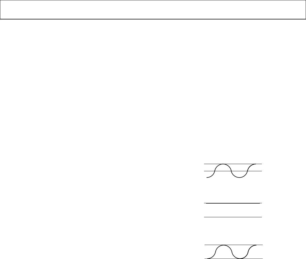
The voltage presented in Figure 20 is shown as sinusoidal for
illustration purposes only. It is meant to represent any voltage
waveform varying between 0 V and some limiting value. The
limiting value can be positive or negative, but the voltage cannot
cross 0 V.
0V
RATED PEAK VOLTAGE
07509-022
Figure 18. Bipolar AC Waveform
0V
RATED PEAK VOLTAGE
07509-024
Figure 19. DC Waveform
0V
RATED PEAK VOLTAGE
07509-023
Figure 20. Unipolar AC Waveform
