Expand menu
Hello, Sign in
My Account
0
Cart
Home
Products
Sensors
Semiconductors
Passive Components
Connectors
Power
Electromechanical
Optoelectronics
Circuit Protection
Integrated Circuits - ICs
Main Products
Manufacturers
Blog
Services
About OMO
About Us
Contact Us
Check Stock
TLE52062SAKSA1
P1-P3
P4-P6
P7-P9
P10-P12
P13-P15
P16-P18
P19-P21
P22-P24
TLE 5206-2
Electrica
l Characteristics
Data Sheet
10
Rev.1.1, 2007-07-31
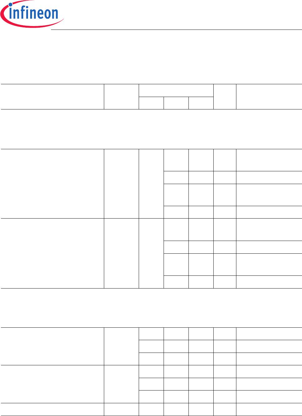
Outputs OUT1, 2
Static Drain-Source
-On Resistance
Source
I
OUT
= – 3 A
R
DS ON
H
–
220
350
m
Ω
6V
<
V
S
< 18
V
T
j
= 25
°
C
–
500
m
Ω
6V
<
V
S
< 18
V
350
500
m
Ω
V
SO
N
<
V
S
≤
6V
T
j
= 25
°
C
–
800
m
Ω
V
SO
N
<
V
S
≤
6V
Sink
I
OUT
= 3 A
R
DS ON
L
–
230
350
m
Ω
6V
<
V
S
<
18 V
T
j
= 25
°
C
–
500
m
Ω
6V
<
V
S
<
18 V
400
600
m
Ω
V
SO
N
<
V
S
≤
6V
T
j
= 25
°
C
–
100
0
m
Ω
V
SO
N
<
V
S
≤
6V
Note:
Values
of
R
DS ON
for
V
S ON
<
V
S
≤
6 V are
guaranteed b
y design.
Overcu
rrent
Source shutdo
wn trippoin
t
–
I
SDH
––1
0
A
T
j
= – 40
°
C
–8–A
T
j
= 25
°
C
6––A
T
j
= 150
°
C
Sink shutdo
wn trippoin
t
I
SDL
––1
0
A
T
j
= – 40
°
C
–8–A
T
j
= 25
°
C
6––A
T
j
= 150
°
C
Shutdown de
lay time
t
dSD
25
50
80
µ
s–
3.3
Electrica
l Characteri
stics
(cont’d)
6 V <
V
S
< 18 V; IN1 = IN2 =
HIGH
I
OUT1
, 2
= 0 A (No lo
ad); – 40
°
C <
T
j
< 150
°
C; u
nless othe
rwise spec
ified
Parameter
Symbol
Limit Values
Unit
Test Condition
min.
typ.
max.
TLE 5206-2
Electrica
l Characteristics
Data Sheet
11
Rev.1.1, 2007-07-31
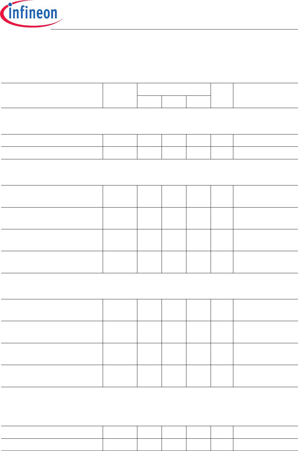
Short Circuit Cur
rent Limitation
Source current
–
I
SCH
––2
0
A
t
< t
dSD
Sink current
I
SCL
––1
5
A
t
< t
dSD
Output Delay Ti
mes (Device
Active for
t
> 1 ms)
Source ON
t
dO
N
H
–1
0
2
0
µ
s
I
OUT
= – 3 A
resistive
load
Sink ON
t
dO
N
L
–1
0
2
0
µ
s
I
OUT
= 3 A
resistive
load
Source OFF
t
dO
F
F
H
–25
µ
s
I
OUT
= – 3 A
resistive
load
Sink OFF
t
dO
F
F
L
–25
µ
s
I
OUT
= 3 A
resistive
load
Output Switching Times (Device Activ
e for
t
> 1 ms)
Source ON
t
ON H
–1
5
3
0
µ
s
I
OUT
= – 3 A
resistive
load
Sink ON
t
ON L
–51
0
µ
s
I
OUT
= 3 A
resistive
load
Source OFF
t
OFF H
–25
µ
s
I
OUT
= – 3 A
resistive
load
Sink OFF
t
OFF L
–25
µ
s
I
OUT
= 3 A
resistive
load
Clamp Diodes
Forward Voltage
High-si
de
V
FH
–11
.
5
V
I
F
= 3 A
Low-side
V
FL
–1
.
1
1
.
5
V
I
F
= 3 A
3.3
Electrica
l Characteri
stics
(cont’d)
6 V <
V
S
< 18 V; IN1 = IN2 =
HIGH
I
OUT1
, 2
= 0 A (No lo
ad); – 40
°
C <
T
j
< 150
°
C; u
nless othe
rwise spec
ified
Parameter
Symbol
Limit Values
Unit
Test Condition
min.
typ.
max.
TLE 5206-2
Electrica
l Characteristics
Data Sheet
12
Rev.1.1, 2007-07-31
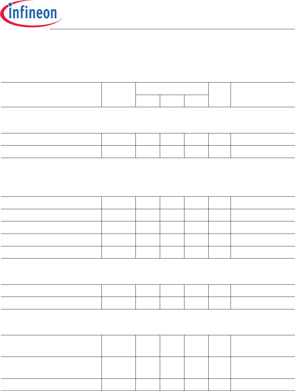
Leakage Curr
ent
Source
I
LKH
– 100
– 35
–
µ
AO
U
T
1
=
V
S
Sink
I
LKL
–
35
100
µ
AO
U
T
2
=
GND
Logic
Control Inputs IN 1, 2
H-input
voltage thre
shold
V
INH
2.8
2.5
–
V
–
L-input volta
ge
V
INL
–1
.
7
1
.
2
V
–
Hys
teresis
of input
volt
age
V
INHY
0.4
0.8
1.2
V
–
H-input curre
nt
I
INH
–2
–
2
µ
A
V
IN
= 5 V
L-input current
I
INL
–1
0
–4
0
µ
A
V
IN
= 0 V
Error Flag Output EF
Low output
voltage
V
EFL
–
0.25
0.5
V
I
EF
= 3 mA
Leakage cu
rrent
I
EFL
––1
0
µ
A
V
EF
= 7 V
Thermal Shutdown
Thermal shutd
own junction
temperatur
e
T
jSD
150
175
200
°
C–
Thermal swi
tch-on junc
tion
temperatur
e
T
jSO
120
–
170
°
C–
Temperatur
e hysteresi
s
∆
T
–3
0
–K
–
Note:
Values
of thermal s
hutdown ar
e guaranteed
by design.
3.3
Electrica
l Characteri
stics
(cont’d)
6 V <
V
S
< 18 V; IN1 = IN2 =
HIGH
I
OUT1
, 2
= 0 A (No lo
ad); – 40
°
C <
T
j
< 150
°
C; u
nless othe
rwise spec
ified
Parameter
Symbol
Limit Values
Unit
Test Condition
min.
typ.
max.
P1-P3
P4-P6
P7-P9
P10-P12
P13-P15
P16-P18
P19-P21
P22-P24
TLE52062SAKSA1
Mfr. #:
Buy TLE52062SAKSA1
Manufacturer:
Infineon Technologies
Description:
Motor / Motion / Ignition Controllers & Drivers POWERTRAIN
Lifecycle:
New from this manufacturer.
Delivery:
DHL
FedEx
Ups
TNT
EMS
Payment:
T/T
Paypal
Visa
MoneyGram
Western
Union
Products related to this Datasheet
TLE52062GAUMA1
TLE52062SAKSA1
TLE5206-2GP
TLE52062AKSA1