TLE 5206-2
Diagnosis
Data Sheet 7 Rev.1.1, 2007-07-31
2 Diagnosis
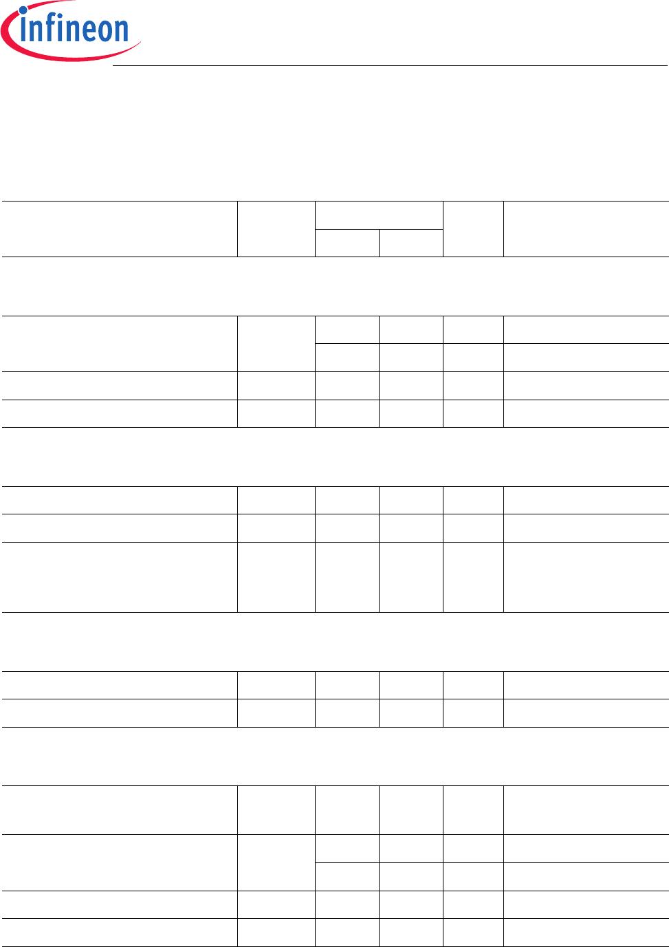
Various errors as listed in the table “Diagnosis” are detected. Short circuits and overload
result in turning off the output stages after a delay
t
dSD
and setting the error flag
simultaneously [EF = L]. Changing the inputs to a state where the fault is not detectable
resets the error flag (input toggling) with the exception of short circuit from OUT1 to
OUT2 (load short circuit).
Flag IN1 IN2 OUT1 OUT2 EF Remarks
Short circuit from OUT1 to OUT2
0
0
1
1
0
1
0
1
L
X
X
H
L
X
X
H
1
0
0
1
Not detectable
Not detectable
Short circuit from OUT1 to GND
0
0
1
1
0
1
0
1
GND
GND
GND
GND
L
X
L
X
1
1
0
0
Not detectable
Not detectable
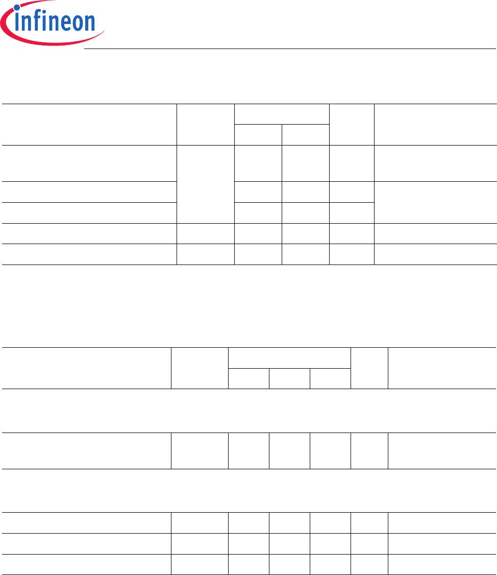
Short circuit from OUT2 to GND
0
0
1
1
0
1
0
1
L
L
X
X
GND
GND
GND
GND
1
0
1
0
Not detectable
Not detectable
Short circuit from OUT1 to
V
S
0
0
1
1
0
1
0
1
V
S
V
S
V
S
V
S
X
H
X
H
0
0
1
1
Not detectable
Not detectable
Short circuit from OUT2 to
V
S
0
0
1
1
0
1
0
1
X
X
H
H
V
S
V
S
V
S
V
S
0
1
0
1
Not detectable
Not detectable
Overtemperature or undervoltage 0
0
1
1
0
1
0
1
Z
Z
Z
Z
Z
Z
Z
Z
0
0
0
0
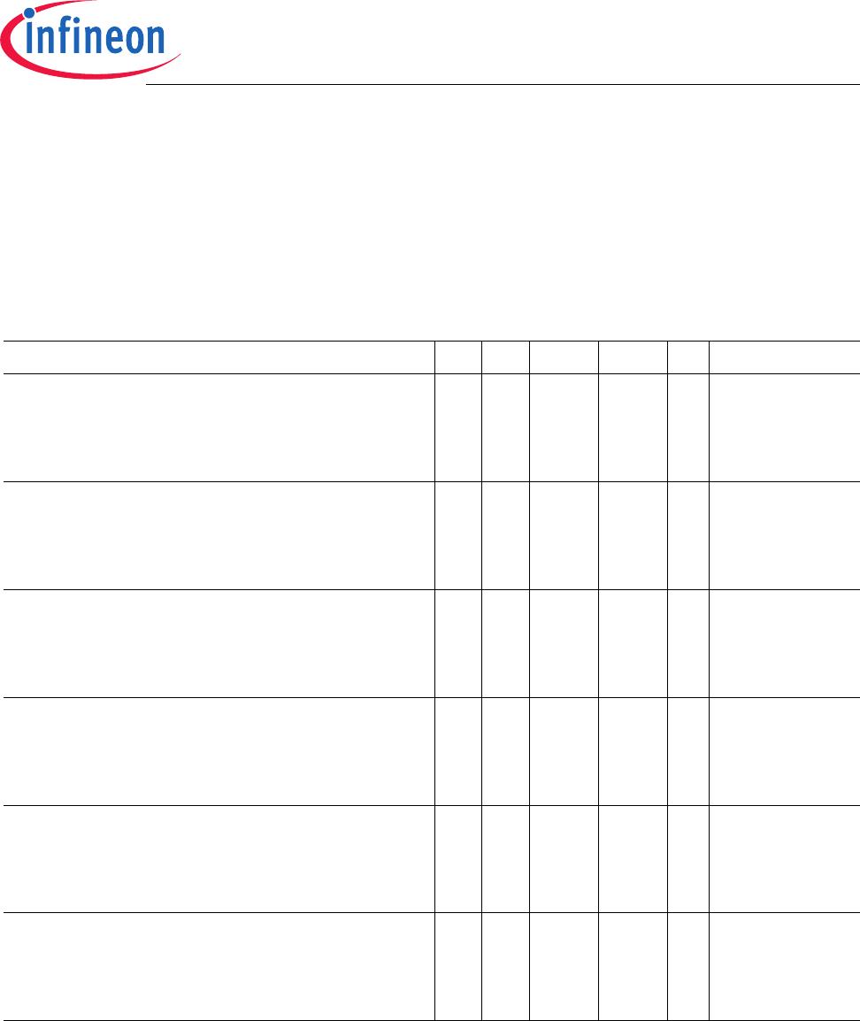
IN: 0 = Logic LOW OUT: Z = Output in tristate condition EF: 1 = No error
1 = Logic HIGH L = Output in sink condition 0 = Error
H = Output in source condition
X = Voltage level undefined
For Open circuit detection, use the TLE 5205-2.
TLE 5206-2
Electrical Characteristics
Data Sheet 8 Rev.1.1, 2007-07-31
3 Electrical Characteristics
Note: Maximum ratings are absolute ratings; exceeding any one of these values may
cause irreversible damage to the integrated circuit.
3.1 Absolute Maximum Ratings
– 40 °C <
T
j
< 150 °C
Parameter Symbol Limit Values Unit Remarks
min. max.
Voltages
Supply voltage
V
S
– 0.3 40 V
– 1 40 V
t < 0.5 s; I
S
> – 5 A
Logic input voltage
V
IN1, 2
– 0.3 7 V 0 V < V
S
< 40 V
Diagnostics output voltage
V
EF
– 0.3 7 V
Currents of DMOS-Transistors and Freewheeling Diodes
Output current (cont.) I
OUT1, 2
– 5 5 A
Output current (peak)
I
OUT1, 2
– 6 6 A t
p
< 100 ms; T =1s
Output current (peak)
I
OUT1, 2
– – A t
p
< 50 µs; T =1s;
internally limitted;
see overcurrent
Temperatures
Junction temperature
T
j
– 40 150 °C–
Storage temperature
T
stg
– 50 150 °C–
Thermal Resistances
Junction case R
thjC
3 K/W P-TO220-7-11/12,
P-TO263-7-1
Junction ambient
R
thjA
65 K/W P-TO220-7-11/12
75 K/W P-TO263-7-1
Junction case
R
thjC
5 K/W PG-DSO-20-37
Junction ambient
R
thjA
50 K/W PG-DSO-20-37
TLE 5206-2
Electrical Characteristics
Data Sheet 9 Rev.1.1, 2007-07-31
3.2 Operating Range
Parameter Symbol Limit Values Unit Remarks
min. max.
Supply voltage
V
S
V
UV ON
40 V After V
S
rising above
V
UV ON
Supply voltage increasing – 0.3 V
UV ON
V Outputs in tristate
condition
Supply voltage decreasing – 0.3
V
UV OFF
V
Logic input voltage
V
IN1, 2
– 0.3 7 V
Junction temperature
T
j
– 40 150 °C–
3.3 Electrical Characteristics
6 V <
V
S
< 18 V; IN1 = IN2 = HIGH
I
OUT1, 2
= 0 A (No load); – 40 °C < T
j
< 150 °C; unless otherwise specified
Parameter Symbol Limit Values Unit Test Condition
min. typ. max.
Current Consumption
Quiescent current
I
S
10 mA IN1 = IN2 = LOW;
V
S
= 13.2 V
Under Voltage Lockout
UV-Switch-ON voltage
V
UV ON
–5.36VV
S
increasing
UV-Switch-OFF voltage
V
UV OFF
3.5 4.7 5.6 V V
S
decreasing
UV-ON/OFF-Hysteresis
V
UV HY
0.2 0.6 V V
UV ON
V
UV OFF

TLE52062SAKSA1

Mfr. #:
Manufacturer:
Infineon Technologies
Description:
Motor / Motion / Ignition Controllers & Drivers POWERTRAIN
Lifecycle:
New from this manufacturer.
Delivery:
DHL FedEx Ups TNT EMS
Payment:
T/T Paypal Visa MoneyGram Western Union

Products related to this Datasheet