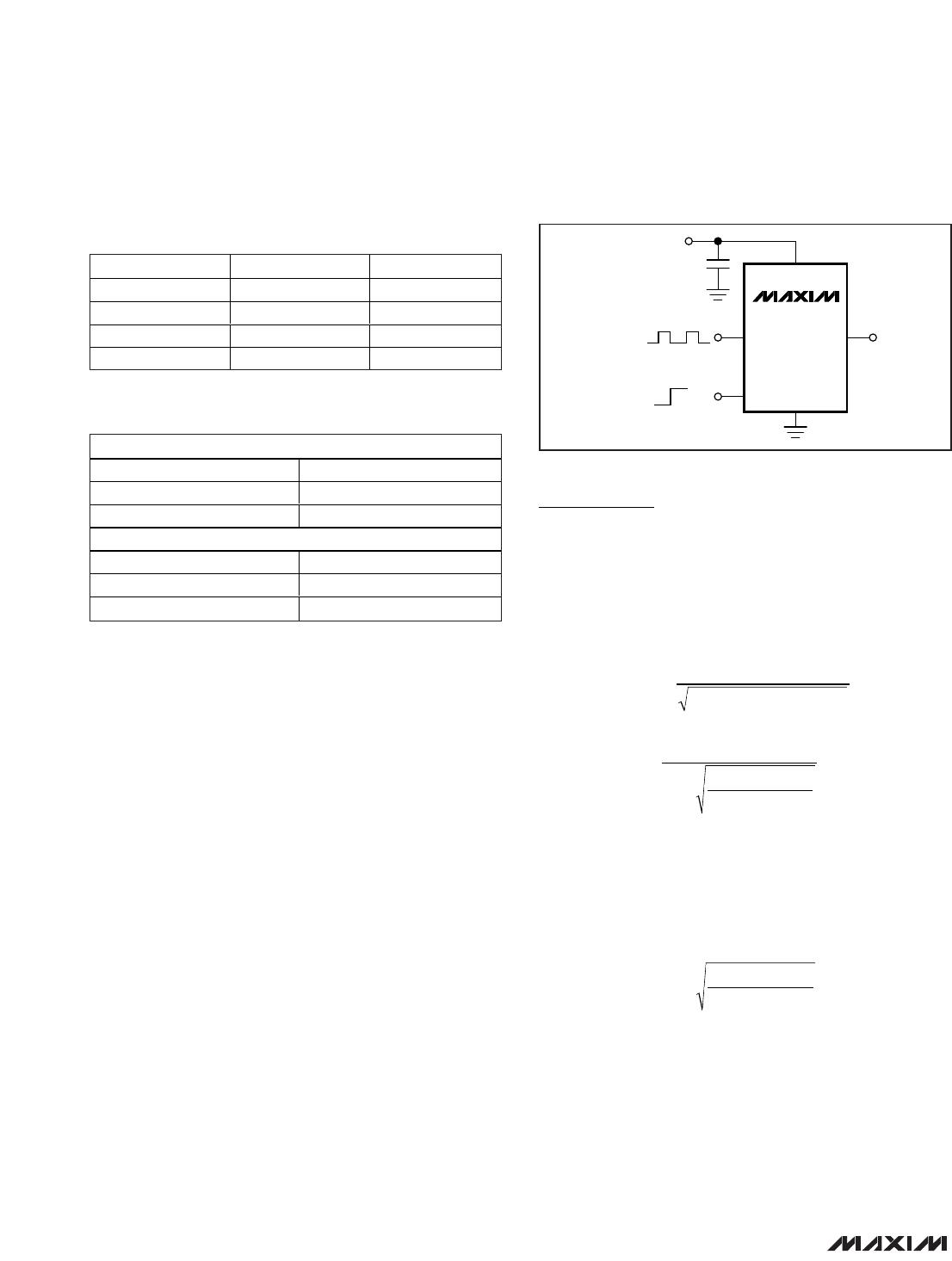
Supply Bypassing and Grounding
Pay extra attention to bypassing and grounding the
MAX5054–MAX5057. Peak supply and output currents
may exceed 8A when both drivers drive large external
capacitive loads in phase. Supply voltage drops and
ground shifts create forms of negative feedback for
inverters and may degrade the delay and transition times.
Ground shifts due to insufficient device grounding may
also disturb other circuits sharing the same AC ground
return path. Any series inductance in the V
DD
, OUT_,
and/or GND paths can cause oscillations due to the very
high di/dt when switching the MAX5054–MAX5057 with
any capacitive load. Place one or more 0.1µF ceramic
capacitors in parallel as close to the device as possible to
bypass V
DD
to GND. Use a ground plane to minimize
ground return resistance and series inductance. Place
the external MOSFET as close as possible to the
MAX5054–MAX5057 to further minimize board induc-
tance and AC path impedance.
Power Dissipation
Power dissipation of the MAX5054–MAX5057 consists
of three components: caused by the quiescent current,
capacitive charge/discharge of internal nodes, and the
output current (either capacitive or resistive load).
Maintain the sum of these components below the maxi-
mum power dissipation limit.
The current required to charge and discharge the internal
nodes is frequency dependent (see the Supply Current
vs. Supply Voltage graph in the
Typical Operating
Characteristics
). The power dissipation (P
Q
) due to the
quiescent switching supply current (I
DD-SW
) per driver
can be calculated as:
P
Q
= V
DD
x I
DD-SW
For capacitive loads, use the following equation to esti-
mate the power dissipation per driver:
P
CLOAD
= C
LOAD
x (V
DD
)
2
x f
SW
where C
LOAD
is the capacitive load, V
DD
is the supply
voltage, and f
SW
is the switching frequency.
Calculate the total power dissipation (P
T
) per driver as
follows:
P
T
= P
Q
+ P
CLOAD
Use the following equation to estimate the MAX5054–
MAX5057 total power dissipation per driver when driving
a ground-referenced resistive load:
P
T
= P
Q
+ P
RLOAD
P
RLOAD
= D x R
ON(MAX)
x I
LOAD
2
where D (duty cycle) is the fraction of the period the
MAX5054–MAX5057’s output pulls high duty cycle,
R
ON(MAX)
is the maximum on-resistance of the device
with the output high, and I
LOAD
is the output load current
of the MAX5054–MAX5057.
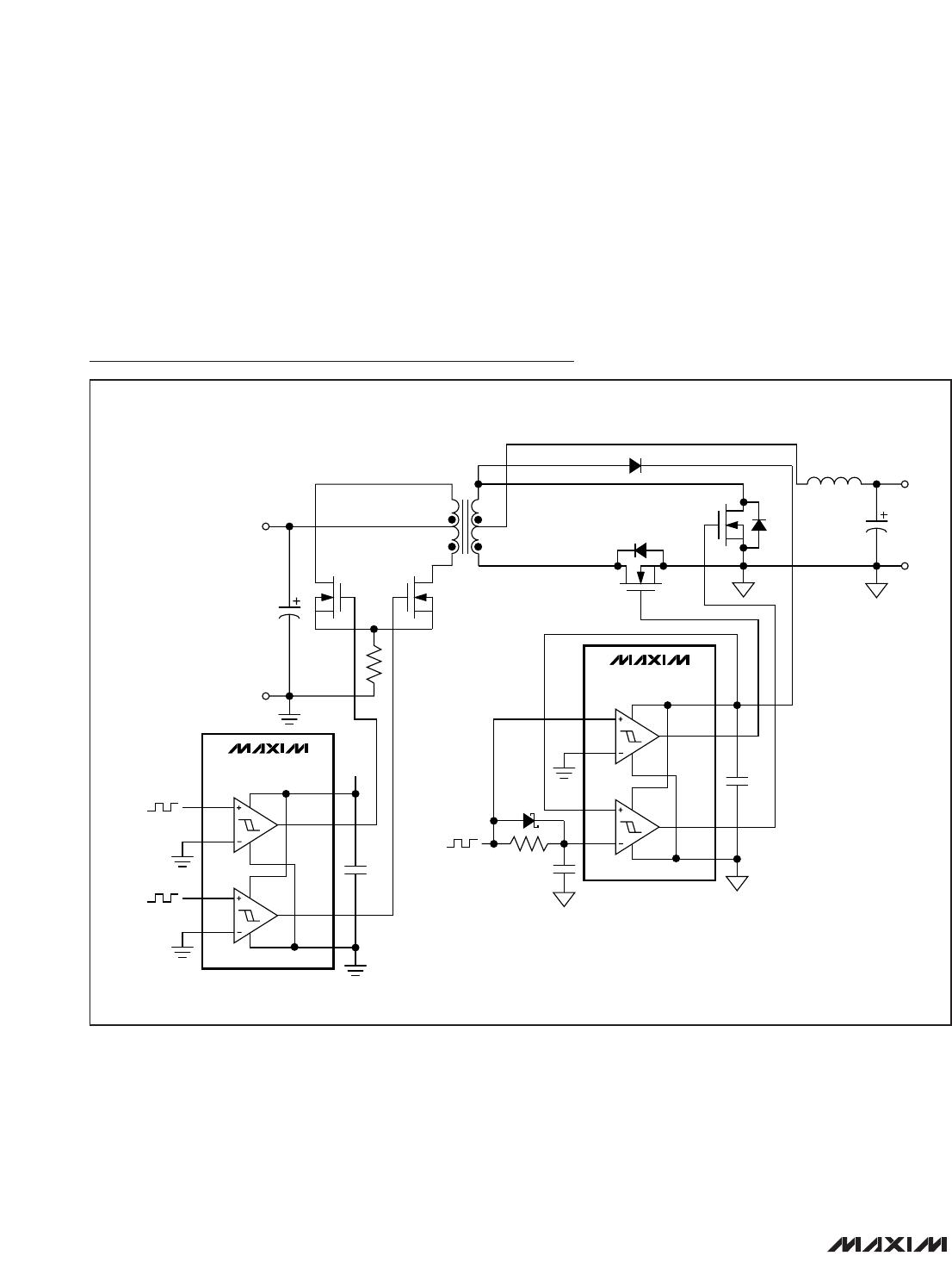
Layout Information
The MAX5054–MAX5057 MOSFET drivers source and
sink large currents to create very fast rising and falling
edges at the gate of the switching MOSFET. The high
di/dt can cause unacceptable ringing if the trace
lengths and impedances are not well controlled. Use the
following PC board layout guidelines when designing
with the MAX5054–MAX5057:
• Place one or more 0.1µF decoupling ceramic
capacitors from V
DD
to GND as close to the device
as possible. Connect V
DD
and GND to large copper
areas. Place one bulk capacitor of 10µF (min) on
the PC board with a low resistance path to the V
DD
input and GND of the MAX5054–MAX5057.
• Two AC current loops form between the device and
the gate of the driven MOSFET. The MOSFET looks
like a large capacitance from gate to source when the
gate pulls low. The active current loop is from the
MOSFET gate to OUT_ of the MAX5054–MAX5057, to
GND of the MAX5054–MAX5057, and to the source of
the MOSFET. When the gate of the MOSFET pulls
high, the active current is from the V
DD
terminal of the
decoupling capacitor, to V
DD
of the MAX5054–
MAX5057, to OUT_ of the MAX5054–MAX5057, to the
MOSFET gate, to the MOSFET source, and to the
negative terminal of the decoupling capacitor. Both
charging current and discharging current loops are
important. Minimize the physical distance and the
impedance in these AC current paths.
• Keep the device as close to the MOSFET as possible.
• In a multilayer PC board, the inner layers should
consist of a GND plane containing the discharging
and charging current loops.
• Pay extra attention to the ground loop and use a
low-impedance source when using a TTL logic-
input device. Fast fall time at OUT_ may corrupt the
input during transition.
MAX5054–MAX5057
4A, 20ns, Dual MOSFET Drivers
______________________________________________________________________________________ 11