Detailed Description
V
DD
Undervoltage Lockout (UVLO)
The MAX5054–MAX5057 have internal undervoltage
lockout for V
DD
. When V
DD
is below the UVLO thresh-
old, OUT_ is low, independent of the state of the inputs.
The undervoltage lockout is typically 3.5V with 200mV
typical hysteresis to avoid chattering. When V
DD
rises
above the UVLO threshold, the outputs go high or low
depending upon the logic-input levels. Bypass V
DD
using low-ESR ceramic capacitors for proper operation
(see the
Applications Information
section).
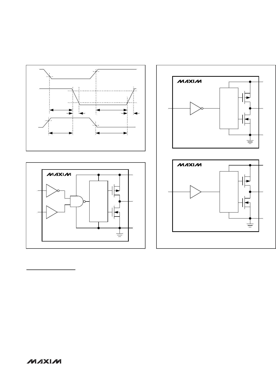
Logic Inputs
The MAX5054B–MAX5057 have TTL-compatible logic
inputs, while the MAX5054A is a CMOS logic-input dri-
ver. The logic-input signals can be independent of the
V
DD
voltage. For example, the device can be powered
by a 5V supply while the logic inputs are provided from
CMOS logic. Also, the logic inputs are protected against
the voltage spikes up to 18V, regardless of the V
DD
volt-
age. The TTL and CMOS logic inputs have 300mV and
0.1 x V
DD
hysteresis, respectively, to avoid possible dou-
ble pulsing during transition. The low 2.5pF input capaci-
tance reduces loading and increases switching speed.
MAX5054–MAX5057
4A, 20ns, Dual MOSFET Drivers
_______________________________________________________________________________________ 9