©2011 Silicon Storage Technology, Inc. DS25080A 11/11
10
2 Mbit SPI Serial Flash
SST25LF020A
Not Recommended for New Designs
A
Microchip Technology Company
Read (20 MHz)
The Read instruction supports up to 20 MHz, it outputs the data starting from the specified address
location. The data output stream is continuous through all addresses until terminated by a low to high
transition on CE#. The internal address pointer will automatically increment until the highest memory
address is reached. Once the highest memory address is reached, the address pointer will automati-
cally increment to the beginning (wrap-around) of the address space, i.e. for 2 Mbit density, once the
data from address location 3FFFFH had been read, the next output will be from address location
00000H.
The Read instruction is initiated by executing an 8-bit command, 03H, followed by address bits [A
23
-
A
0
]. CE# must remain active low for the duration of the Read cycle. See Figure 5 for the Read
sequence.
Figure 5: Read Sequence
7. Block addresses for: use A
MS
-A
15
, remaining addresses can be V
IL
or V
IH
8. To continue programming to the next sequential address location, enter the 8-bit command, AFH,
followed by the data to be programmed.
9. The Read-Status-Register is continuous with ongoing clock cycles until terminated by a low to high transition on CE#.
10. The Enable-Write-Status-Register (EWSR) instruction and the Write-Status-Register (WRSR) instruction must work in
conjunction of each other. The WRSR instruction must be executed immediately (very next bus cycle) after the EWSR
instruction to make both instructions effective.
11. Manufacturer’s ID is read with A
0
=0, and Device ID is read with A
0
=1. All other address bits are 00H. The Manufacturer
and Device ID output stream is continuous until terminated by a low to high transition on CE#
12. Device ID = 43H for SST25LF020A
1242 F04.0
CE#
SO
SI
SCK
ADD.
012345678
ADD. ADD.
03
HIGH IMPEDANCE
15 16
23
24
31
32
39
40
7047 48 55 56 63 64
N+2 N+3 N+4N N+1
D
OUT
MSB
MSB
MSB
MODE 0
MODE 3
D
OUT
D
OUT
D
OUT
D
OUT
©2011 Silicon Storage Technology, Inc. DS25080A 11/11
11
2 Mbit SPI Serial Flash
SST25LF020A
Not Recommended for New Designs
A
Microchip Technology Company
High-Speed-Read (33 MHz)
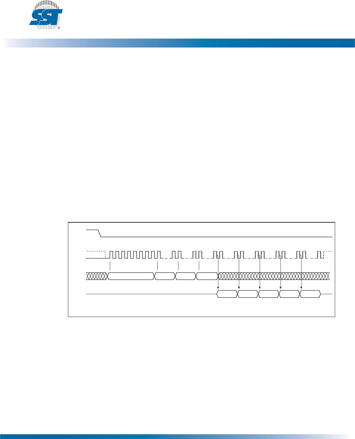
The High-Speed-Read instruction supporting up to 33 MHz is initiated by executing an 8-bit command,
0BH, followed by address bits [A
23
-A
0
] and a dummy byte. CE# must remain active low for the duration
of the High-Speed-Read cycle. See Figure 6 for the High-Speed-Read sequence.
Following a dummy byte (8 clocks input dummy cycle), the High-Speed-Read instruction outputs the
data starting from the specified address location. The data output stream is continuous through all
addresses until terminated by a low to high transition on CE#. The internal address pointer will auto-
matically increment until the highest memory address is reached. Once the highest memory address is
reached, the address pointer will automatically increment to the beginning (wrap-around) of the
address space, i.e. for 2 Mbit density, once the data from address location 03FFFFH has been read,
the next output will be from address location 000000H.
Figure 6: High-Speed-Read Sequence
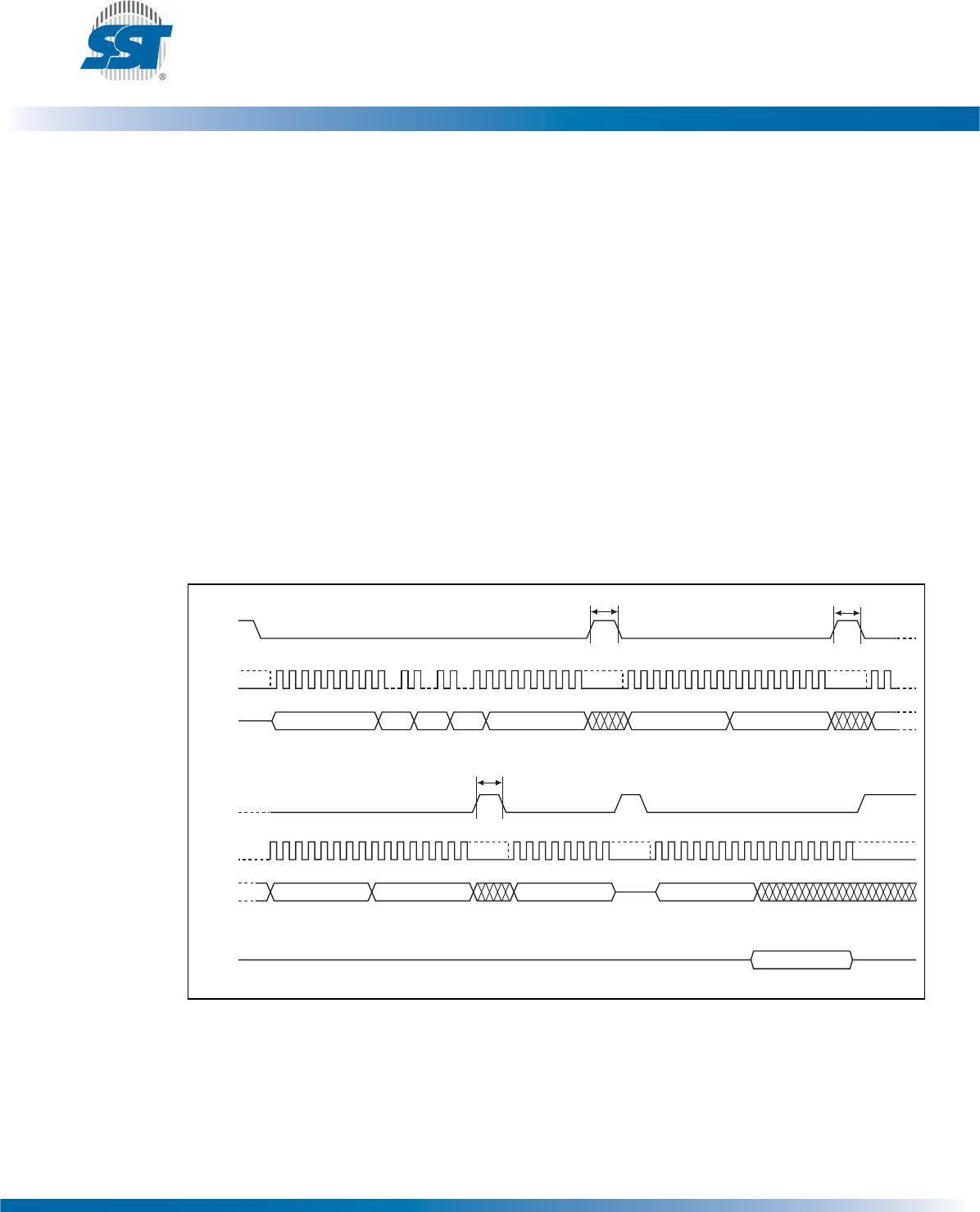
Byte-Program
The Byte-Program instruction programs the bits in the selected byte to the desired data. The selected
byte must be in the erased state (FFH) when initiating a Program operation. A Byte-Program instruction
applied to a protected memory area will be ignored.
Prior to any Write operation, the Write-Enable (WREN) instruction must be executed. CE# must remain
active low for the duration of the Byte-Program instruction. The Byte-Program instruction is initiated by
executing an 8-bit command, 02H, followed by address bits [A
23
-A
0
]. Following the address, the data is
input in order from MSB (bit 7) to LSB (bit 0). CE# must be driven high before the instruction is exe-
cuted. The user may poll the Busy bit in the software status register or wait T
BP
for the completion of
the internal self-timed Byte-Program operation. See Figure 7 for the Byte-Program sequence.
Figure 7: Byte-Program Sequence
1242 F05.0
CE#
SO
SI
SCK
ADD.
012345678
ADD. ADD.0B
HIGH IMPEDANCE
15 16 23 24 31 32 39 40
47 48 55 56 63 64
N+2 N+3 N+4
N
N+1
X
MSB
MSB
MSB
MODE 0
MODE 3
D
OUT
D
OUT
D
OUT
D
OUT
80
71 72
D
OUT
Note: X = Dummy Byte: 8 Clocks Input Dummy Cycle (V
IL
or V
IH
)
1242 F06.0
CE#
SO
SI
SCK
ADD.
012345678
ADD. ADD. D
IN
02
HIGH IMPEDANCE
15 16
23
24
31
32
39
MODE 0
MODE 3
MSBMSB
MSB
LSB
©2011 Silicon Storage Technology, Inc. DS25080A 11/11
12
2 Mbit SPI Serial Flash
SST25LF020A
Not Recommended for New Designs
A
Microchip Technology Company
Auto Address Increment (AAI) Program
The AAI program instruction allows multiple bytes of data to be programmed without re-issuing the
next sequential address location. This feature decreases total programming time when the entire mem-
ory array is to be programmed. An AAI program instruction pointing to a protected memory area will be
ignored. The selected address range must be in the erased state (FFH) when initiating an AAI program
instruction.
Prior to any write operation, the Write-Enable (WREN) instruction must be executed. The AAI program
instruction is initiated by executing an 8-bit command, AFH, followed by address bits [A
23
-A
0
]. Follow-
ing the addresses, the data is input sequentially from MSB (bit 7) to LSB (bit 0). CE# must be driven
high before the AAI program instruction is executed. The user must poll the BUSY bit in the software
status register or wait T
BP
for the completion of each internal self-timed Byte-Program cycle. Once the
device completes programming byte, the next sequential address may be program, enter the 8-bit
command, AFH, followed by the data to be programmed. When the last desired byte had been pro-
grammed, execute the Write-Disable (WRDI) instruction, 04H, to terminate AAI. After execution of the
WRDI command, the user must poll the Status register to ensure the device completes programming.
See Figure 8 for AAI programming sequence.
There is no wrap mode during AAI programming; once the highest unprotected memory address is
reached, the device will exit AAI operation and reset the Write-Enable-Latch bit (WEL = 0).
Figure 8: Auto Address Increment (AAI) Program Sequence
CE#
SI
SCK
A[23:16] A[15:8] A[7:0]
AF
Data Byte 1
AF
DataByte2
CE#
SI
SO
SCK
Write Disable (WRDI)
Instruction to terminate
AAI Operation
Read Status Register (RDSR)
Instruction to verify end of
AAI Operation
04Last Data ByteAF
05
D
OUT
MODE 3
MODE 0
T
BP
T
BP
T
BP
1242 F07.0
012345678 32333435363738391516 2324 31 0123456789101112131415 01
012345670123456789101112131415 0123456789101112131415

SST25LF020A-33-4I-QAE

Mfr. #:
Manufacturer:
Microchip Technology
Description:
NOR Flash 2Mbit 33MHz
Lifecycle:
New from this manufacturer.
Delivery:
DHL FedEx Ups TNT EMS
Payment:
T/T Paypal Visa MoneyGram Western Union